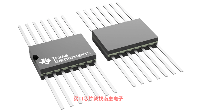
- 制造厂商:TI
- 产品类别:逻辑和电压转换
- 技术类目:逻辑门 - 与非门
- 功能描述:航天类 4 通道、2 输入、2V 至 3.6V 与非门
- 点击这里打开及下载SN54LVC00A-SP的技术文档资料
- TI代理渠道,提供当日发货、严格的质量标准,满足您的目标价格

The SN54LVC00A quadruple 2-input positive-NAND gate is designed for 2.7-V to 3.6-V VCC operation, and the SN74LVC00A quadruple 2-input positive-NAND gate is designed for 1.65-V to 3.6-V VCC operation.
The SNx4LVC00A devices perform the Boolean function Y = A × B or Y = A + B in positive logic.
Inputs can be driven from either 3.3-V or 5-V devices. This feature allows the use of these devices as translators in a mixed 3.3-V/5-V system environment.
- Operate From 1.65 V to 3.6 V
- Specified From –40°C to 85°C, –40°C to 125°C, and –55°C to 125°C
- Inputs Accept Voltages to 5.5 V
- Max tpd of 4.3 ns at 3.3 V
- Typical VOLP (Output Ground Bounce) < 0.8 V at VCC = 3.3 V, TA = 25°C
- Typical VOHV (Output VOH Undershoot) > 2 V at VCC = 3.3 V, TA = 25°C
- Latch-Up Performance Exceeds 250 mA Per JESD 17
- On Products Compliant to MIL-PRF-38535, All Parameters Are Tested Unless Otherwise Noted. On All Other Products, Production Processing Does Not Necessarily Include Testing of All Parameters.
- ESD Protection Exceeds JESD 22
- 2000-V Human-Body Model
- 200-V Machine Model
- 1000-V Charged-Device Model
- Technology Family
- LVC
- Supply voltage (Min) (V)
- 2
- Supply voltage (Max) (V)
- 3.6
- Number of channels (#)
- 4
- Inputs per channel
- 2
- IOL (Max) (mA)
- 24
- IOH (Max) (mA)
- -24
- Input type
- Standard CMOS
- Output type
- Push-Pull
- Features
- Partial power down (Ioff), Over-voltage tolerant inputs, Ultra high speed (tpd <5ns)
- Data rate (Max) (Mbps)
- 100
- Rating
- Space
SN54LVC00A-SP的完整型号有:5962-9753301VDA,以下是这些产品的关键参数及官网采购报价:
5962-9753301VDA,工作温度:-55 to 125,封装:CFP (W)-14,包装数量MPQ:1个,MSL 等级/回流焊峰值温度:N/A for Pkg Type,引脚镀层/焊球材料:SNPB,TI官网5962-9753301VDA的批量USD价格:197.264(1000+)

5962-9753301VDA,工作温度:-55 to 125,封装:CFP (W)-14,包装数量MPQ:1个,MSL 等级/回流焊峰值温度:N/A for Pkg Type,引脚镀层/焊球材料:SNPB,TI官网5962-9753301VDA的批量USD价格:197.264(1000+)


