- 制造厂商:TI
- 产品类别:接口
- 技术类目:CAN、LIN 收发器和 SBC
- 功能描述:高温 3.3V CAN 收发器
- 点击这里打开及下载SN65HVD233-HT的技术文档资料
- TI代理渠道,提供当日发货、严格的质量标准,满足您的目标价格

The SN65HVD233 is used in applications employing the controller area network (CAN) serial communication physical layer in accordance with the ISO 11898 standard, with the exception that the thermal shutdown is removed. As a CAN transceiver, the device provides transmit and receive capability between the differential CAN bus and a CAN controller, with signaling rates up to 1 Mbps.
Designed for operation in especially harsh environments, the device features cross wire, overvoltage, and loss-of-ground protection to ±36 V, with common-mode transient protection of ±100 V. This device operates over a –7-V to 12-V common-mode range with a maximum of 60 nodes on a bus.
If the common-mode range is restricted to the ISO 11898 standard range of –2 V to 7 V, up to 120 nodes may be connected on a bus. This transceiver interfaces the single-ended CAN controller with the differential CAN bus found in industrial, building automation, and automotive applications.
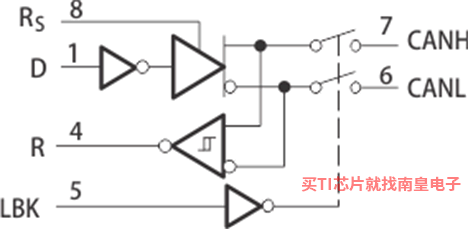
RS (pin 8) provides for three modes of operation: high-speed, slope control, or low-power standby mode. The high-speed mode of operation is selected by connecting RS directly to ground, thus allowing the driver output transistors to switch on and off as fast as possible with no limitation on the rise and fall slope. The rise and fall slope can be adjusted by connecting a resistor to ground at RS, because the slope is proportional to the output current of the pin. Slope control is implemented with a resistor value of 10 kΩ to achieve a slew rate of ? 15 V/µs, and a value of 100 kΩ to achieve ? 2 V/µs slew rate. For more information about slope control, refer to the Application and Implementation section.
The SN65HVD233 enters a low-current standby mode, during which the driver is switched off and the receiver remains active if a high logic level is applied to RS. The local protocol controller reverses this low-current standby mode when it needs to transmit to the bus.
A logic high on the loopback (LBK, pin 5) of the SN65HVD233 places the bus output and bus input in a high-impedance state. The remaining circuit remains active and available for the driver to receiver loopback, self-diagnostic node functions without disturbing the bus.
- Bus-Pin Fault Protection Exceeds ±36 V
- Bus-Pin ESD Protection Exceeds 16-kV Human Body Model (HBM)
- Compatible With ISO 11898
- Signaling Rates(1) up to 1 Mbps
- Extended –7-V to 12-V Common-Mode Range
- High-Input Impedance Allows for 120 Nodes
- LVTTL I/Os Are 5-V Tolerant
- Adjustable Driver Transition Times for Improved Signal Quality
- Unpowered Node Does Not Disturb the Bus
- Low-Current Standby Mode: 200 μA Typical
- Power-Up and Power-Down Glitch-Free Bus Inputs and Outputs
- High-Input Impedance With Low VCC
- Monolithic Output During Power Cycling
- Loopback for Diagnostic Functions Available
- DeviceNet? Vendor ID #806(1)
- APPLICATIONS
- Down-Hole Drilling
- High-Temperature Environments
- Industrial Automation
- DeviceNet Data Buses
- Smart Distributed Systems (SDS?)
- SAE J1939 Data Bus Interfaces
- NMEA 2000 Data Bus Interfaces
- ISO 11783 Data Bus Interfaces
- CAN Data Bus Interfaces
- Controlled Baseline
- One Assembly or Test Site
- One Fabrication Site
- Available in Extreme (–55°C to 210°C) Temperature Range2
- Extended Product Life Cycle
- Extended Product-Change Notification
- Product Traceability
- Texas Instruments high-temperature products use highly optimized silicon (die) solutions with design and process enhancements to maximize performance over extended temperatures.
(1) The signaling rate of a line is the number of voltage transitions that are made per second expressed in the units bps (bits per second). 2 Custom temperature ranges available All other trademarks are the property of their respective owners
- Protocols
- CAN
- Number of channels (#)
- 1
- Supply voltage (V)
- 3 to 3.6
- Bus fault voltage (V)
- -36 to 36
- Signaling rate (Max) (Mbps)
- 1
- Rating
- High Temp
- Operating temperature range (C)
- -55 to 175, -55 to 210
- Low power mode
- Silent
- Common mode voltage (V)
- -7 to 12
- Isolated
- No
SN65HVD233-HT的完整型号有:SN65HVD233HD、SN65HVD233SHKJ、SN65HVD233SHKQ、SN65HVD233SJD、SN65HVD233SKGDA,以下是这些产品的关键参数及官网采购报价:
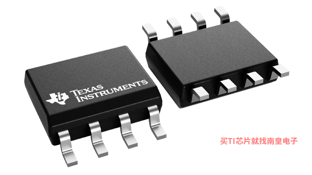
SN65HVD233HD,工作温度:-55 to 175,封装:SOIC (D)-8,包装数量MPQ:75个,MSL 等级/回流焊峰值温度:Level-1-260C-UNLIM,引脚镀层/焊球材料:NIPDAU,TI官网SN65HVD233HD的批量USD价格:78.538(1000+)
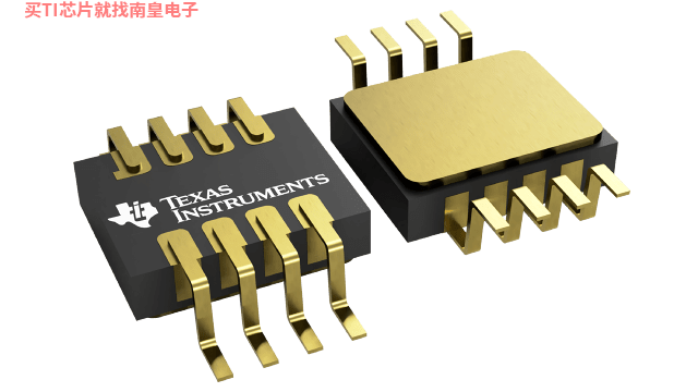
SN65HVD233SHKJ,工作温度:-55 to 210,封装:CFP (HKJ)-8,包装数量MPQ:25个,MSL 等级/回流焊峰值温度:N/A for Pkg Type,引脚镀层/焊球材料:Call TI,TI官网SN65HVD233SHKJ的批量USD价格:78.538(1000+)
SN65HVD233SHKQ,工作温度:-55 to 210,封装:CFP (HKQ)-8,包装数量MPQ:25个,MSL 等级/回流焊峰值温度:N/A for Pkg Type,引脚镀层/焊球材料:AU,TI官网SN65HVD233SHKQ的批量USD价格:78.538(1000+)
SN65HVD233SJD,工作温度:-55 to 210,封装:CDIP SB (JDJ)-8,包装数量MPQ:37个,MSL 等级/回流焊峰值温度:N/A for Pkg Type,引脚镀层/焊球材料:Call TI,TI官网SN65HVD233SJD的批量USD价格:78.538(1000+)
SN65HVD233SKGDA,工作温度:-55 to 210,封装: (KGD)-0,包装数量MPQ:130个,MSL 等级/回流焊峰值温度:N/A for Pkg Type,引脚镀层/焊球材料:Call TI,TI官网SN65HVD233SKGDA的批量USD价格:42.126(1000+)

HEATEVM GUI Software (Rev. A)
PSpice for TI 可提供帮助评估模拟电路功能的设计和仿真环境。此功能齐全的设计和仿真套件使用 Cadence 的模拟分析引擎。PSpice for TI 可免费使用,包括业内超大的模型库之一,涵盖我们的模拟和电源产品系列以及精选的模拟行为模型。借助?PSpice for TI 的设计和仿真环境及其内置的模型库,您可对复杂的混合信号设计进行仿真。创建完整的终端设备设计和原型解决方案,然后再进行布局和制造,可缩短产品上市时间并降低开发成本。
在?PSpice for TI 设计和仿真工具中,您可以搜索 TI (...)
TINA-TI — 基于 SPICE 的模拟仿真程序
TINA-TI 提供了 SPICE 所有的传统直流、瞬态和频域分析以及更多。TINA 具有广泛的后处理功能,允许您按照希望的方式设置结果的格式。虚拟仪器允许您选择输入波形、探针电路节点电压和波形。TINA 的原理图捕获非常直观 - 真正的“快速入门”。TINA-TI 安装需要大约 500MB。直接安装,如果想卸载也很容易。我们相信您肯定会爱不释手。
TINA 是德州仪器 (TI) 专有的 DesignSoft 产品。该免费版本具有完整的功能,但不支持完整版 TINA 所提供的某些其他功能。
如需获取可用 TINA-TI 模型的完整列表,请参阅:SpiceRack - 完整列表
需要 HSpice (...)
TIDA-00002 — 针对高温应用的苛刻环境采集终端 (HEAT) EVM 平台
HEATEVM 是旨在为信号调节和处理器评估提供高温平台的 MCM。该模块包含完整的组件链,这些组件设计为可禁受高达 200 °C 的极端工作温度。PCB 采用也适用于这些极端温度的聚酰亚胺材料制成。