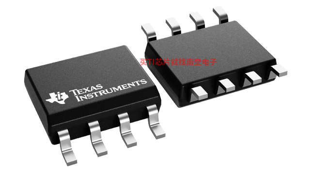
- 制造厂商:TI
- 产品类别:接口
- 技术类目:RS-485 和 RS-422 收发器
- 功能描述:汽车类差动总线收发器
- 点击这里打开及下载SN65LBC176-Q1的技术文档资料
- TI代理渠道,提供当日发货、严格的质量标准,满足您的目标价格

The SN65LBC176 differential bus transceiver is a monolithic, integrated circuit designed for bidirectional data communication on multipoint bus-transmission lines. It is designed for balanced transmission lines and meets ANSI Standard RS-485 and ISO 8482:1987(E).
The SN65LBC176 combines a 3-state, differential line driver and a differential input line receiver, both of which operate from a single 5-V power supply. The driver and receiver have active-high and active-low enables, respectively, which can externally connect together to function as a direction control. The driver differential outputs and the receiver differential inputs connect internally to form a differential input/output (I/O) bus port that is designed to offer minimum loading to the bus whenever the driver is disabled or VCC = 0. This port features wide positive and negative common-mode voltage ranges, making the device suitable for party-line applications. Very low device supply current can be achieved by disabling the driver and the receiver. Both the driver and receiver are available as cells in the Texas Instruments LinASIC™ Library.
This transceiver is suitable for ANSI Standard RS-485 and ISO 8482:1987 (E) applications to the extent that they are specified in the operating conditions and characteristics section of this data sheet. Certain limits contained in the ANSI Standard RS-485 and ISO 8482:1987 (E) are not met or cannot be tested over the entire extended temperature range.
- Qualified for Automotive Applications
- Bidirectional Transceiver
- Meet or Exceed the Requirements of ANSI Standard RS-485 and ISO 8482:1987(E)
- High-Speed Low-Power LinBiCMOS? Circuitry
- Designed for High-Speed Operation in Both Serial and Parallel Applications
- Low Skew
- Designed for Multipoint Transmission on Long Bus Lines in Noisy Environments
- Very Low Disabled Supply-Current Requirements . . . 200 μA Maximum
- Wide Positive and Negative Input/Output Bus Voltage Ranges
- Driver Output Capacity . . . ±60 mA
- Thermal-Shutdown Protection
- Driver Positive-and Negative-Current Limiting
- Open-Circuit Fail-Safe Receiver Design
- Receiver Input Sensitivity . . . ±200 mV Max
- Receiver Input Hysteresis . . . 50 mV Typ
- Operate From a Single 5-V Supply
- Glitch-Free Power-Up and Power-Down Protection
LinBiCMOS and LinASIC are trademarks of Texas Instruments Incorporated.
- Number of receivers
- 1
- Number of transmitters
- 1
- Duplex
- Half
- Supply voltage (Nom) (V)
- 5
- Signaling rate (Max) (Mbps)
- 10
- IEC 61000-4-2 contact (+/- kV)
- ―
- Fault protection (V)
- -10 to 15
- Common mode range
- -7 to 12
- Number of nodes
- 32
- Isolated
- No
- ICC (Max) (mA)
- 1.75
- Rating
- Automotive
- Operating temperature range (C)
- -40 to 125
SN65LBC176-Q1的完整型号有:SN65LBC176QDRG4Q1、SN65LBC176QDRQ1,以下是这些产品的关键参数及官网采购报价:
SN65LBC176QDRG4Q1,工作温度:-40 to 125,封装:SOIC (D)-8,包装数量MPQ:2500个,MSL 等级/回流焊峰值温度:Level-1-260C-UNLIM,引脚镀层/焊球材料:NIPDAU,TI官网SN65LBC176QDRG4Q1的批量USD价格:1.381(1000+)
SN65LBC176QDRQ1,工作温度:-40 to 125,封装:SOIC (D)-8,包装数量MPQ:2500个,MSL 等级/回流焊峰值温度:Level-1-260C-UNLIM,引脚镀层/焊球材料:NIPDAU,TI官网SN65LBC176QDRQ1的批量USD价格:1.231(1000+)

PSPICE-FOR-TI ― 适用于 TI 设计和模拟工具的 PSpice
PSpice for TI 可提供帮助评估模拟电路功能的设计和仿真环境。此功能齐全的设计和仿真套件使用 Cadence 的模拟分析引擎。PSpice for TI 可免费使用,包括业内超大的模型库之一,涵盖我们的模拟和电源产品系列以及精选的模拟行为模型。借助?PSpice for TI 的设计和仿真环境及其内置的模型库,您可对复杂的混合信号设计进行仿真。创建完整的终端设备设计和原型解决方案,然后再进行布局和制造,可缩短产品上市时间并降低开发成本。
在?PSpice for TI 设计和仿真工具中,您可以搜索 TI (...)
TINA-TI ― 基于 SPICE 的模拟仿真程序
TINA-TI 提供了 SPICE 所有的传统直流、瞬态和频域分析以及更多。TINA 具有广泛的后处理功能,允许您按照希望的方式设置结果的格式。虚拟仪器允许您选择输入波形、探针电路节点电压和波形。TINA 的原理图捕获非常直观 - 真正的“快速入门”。TINA-TI 安装需要大约 500MB。直接安装,如果想卸载也很容易。我们相信您肯定会爱不释手。
TINA 是德州仪器 (TI) 专有的 DesignSoft 产品。该免费版本具有完整的功能,但不支持完整版 TINA 所提供的某些其他功能。
如需获取可用 TINA-TI 模型的完整列表,请参阅:SpiceRack - 完整列表
需要 HSpice (...)


