- 制造厂商:TI
- 产品类别:接口
- 技术类目:LVDS、M-LVDS 和 PECL IC
- 功能描述:半双工 LVDM 收发器
- 点击这里打开及下载SN65LVDM176的技术文档资料
- TI代理渠道,提供当日发货、严格的质量标准,满足您的目标价格

The SN65LVDM176 is a differential line driver and receiver configured as a transceiver that uses low-voltage differential signaling (LVDS) to achieve signaling rates as high as 400 Mbit/s. These circuits are similar to TIA/EIA-644 standard compliant devices (SN65LVDS) counterparts except that the output current of the drivers is doubled. This modification provides a minimum differential output voltage magnitude of 247 mV into a 50- load and allows double-terminated lines and half-duplex operation. The receivers detect a voltage difference of less than 50 mV with up to 1 V of ground potential difference between a transmitter and receiver.
The intended application of this device and signaling technique is for half-duplex or multiplex baseband data transmission over controlled impedance media of approximately 100- characteristic impedance. The transmission media may be printed-circuit board traces, backplanes, or cables. (Note: The ultimate rate and distance of data transfer is dependent upon the attenuation characteristics of the media, the noise coupling to the environment, and other application specific characteristics).
The SN65LVDM176 is characterized for operation from \x9640°C to 85°C.
- Low-Voltage Differential Driver and Receiver for Half-Duplex Operation
- Designed for Signaling Rates of 400 Mbit/s
- ESD Protection Exceeds 15 kV on Bus Pins
- Operates From a Single 3.3-V Supply
- Low-Voltage Differential Signaling With Typical Output Voltages of 350 mV and a 50- Load
- Valid Output With as Little as 50 mV Input Voltage Difference
- Propagation Delay Times
- Driver: 1.7 ns Typ
- Receiver: 3.7 ns Typ
- Power Dissipation at 200 MHz
- Driver: 50 mW Typical
- Receiver: 60 mW Typical
- LVTTL Levels Are 5-V Tolerant
- Bus Pins Are High Impedance When Disabled or With VCC Less Than 1.5 V
- Open-Circuit Fail-Safe Receiver
- Surface-Mount Packaging
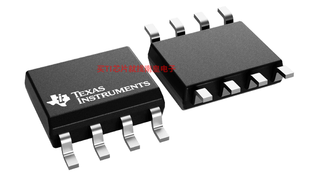
- D Package (SOIC)
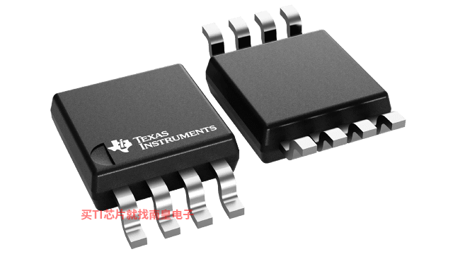
- DGK Package (MSOP)
PowerPAD is a trademark of Texas Instruments.
- Function
- Transceiver
- Protocols
- LVDM, LVDS
- Number of transmitters
- 1
- Number of receivers
- 1
- Supply voltage (V)
- 3.3
- Signaling rate (Mbps)
- 400
- Input signal
- LVDM, LVTTL
- Output signal
- LVDM, LVTTL
- Rating
- Catalog
- Operating temperature range (C)
- -40 to 85
SN65LVDM176的完整型号有:SN65LVDM176D、SN65LVDM176DGK、SN65LVDM176DGKR、SN65LVDM176DR,以下是这些产品的关键参数及官网采购报价:
SN65LVDM176D,工作温度:-40 to 85,封装:SOIC (D)-8,包装数量MPQ:75个,MSL 等级/回流焊峰值温度:Level-1-260C-UNLIM,引脚镀层/焊球材料:NIPDAU,TI官网SN65LVDM176D的批量USD价格:2.016(1000+)
SN65LVDM176DGK,工作温度:-40 to 85,封装:VSSOP (DGK)-8,包装数量MPQ:80个,MSL 等级/回流焊峰值温度:Level-1-260C-UNLIM,引脚镀层/焊球材料:NIPDAUAG,TI官网SN65LVDM176DGK的批量USD价格:2.016(1000+)
SN65LVDM176DGKR,工作温度:-40 to 85,封装:VSSOP (DGK)-8,包装数量MPQ:2500个,MSL 等级/回流焊峰值温度:Level-1-260C-UNLIM,引脚镀层/焊球材料:NIPDAUAG,TI官网SN65LVDM176DGKR的批量USD价格:1.872(1000+)
SN65LVDM176DR,工作温度:-40 to 85,封装:SOIC (D)-8,包装数量MPQ:2500个,MSL 等级/回流焊峰值温度:Level-1-260C-UNLIM,引脚镀层/焊球材料:NIPDAU,TI官网SN65LVDM176DR的批量USD价格:1.872(1000+)

SN65LVDM176 IBIS Model
PSpice for TI 可提供帮助评估模拟电路功能的设计和仿真环境。此功能齐全的设计和仿真套件使用 Cadence 的模拟分析引擎。PSpice for TI 可免费使用,包括业内超大的模型库之一,涵盖我们的模拟和电源产品系列以及精选的模拟行为模型。借助?PSpice for TI 的设计和仿真环境及其内置的模型库,您可对复杂的混合信号设计进行仿真。创建完整的终端设备设计和原型解决方案,然后再进行布局和制造,可缩短产品上市时间并降低开发成本。
在?PSpice for TI 设计和仿真工具中,您可以搜索 TI (...)
TINA-TI ― 基于 SPICE 的模拟仿真程序
TINA-TI 提供了 SPICE 所有的传统直流、瞬态和频域分析以及更多。TINA 具有广泛的后处理功能,允许您按照希望的方式设置结果的格式。虚拟仪器允许您选择输入波形、探针电路节点电压和波形。TINA 的原理图捕获非常直观 - 真正的“快速入门”。TINA-TI 安装需要大约 500MB。直接安装,如果想卸载也很容易。我们相信您肯定会爱不释手。
TINA 是德州仪器 (TI) 专有的 DesignSoft 产品。该免费版本具有完整的功能,但不支持完整版 TINA 所提供的某些其他功能。
如需获取可用 TINA-TI 模型的完整列表,请参阅:SpiceRack - 完整列表
需要 HSpice (...)


