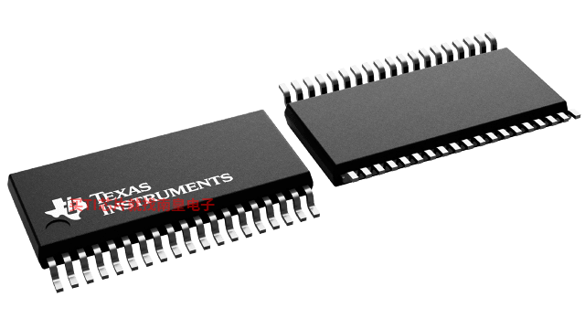
- 制造厂商:TI
- 产品类别:接口
- 技术类目:LVDS、M-LVDS 和 PECL IC
- 功能描述:1:8 LVDS 时钟扇出缓冲器
- 点击这里打开及下载SN65LVDS108的技术文档资料
- TI代理渠道,提供当日发货、严格的质量标准,满足您的目标价格

The SN65LVDS108 is configured as one differential line receiver connected to eight differential line drivers. Individual output enables are provided for each output and an additional enable is provided for all outputs.
The line receivers and line drivers implement the electrical characteristics of low-voltage differential signaling (LVDS). LVDS, as specified in EIA/TIA-644, is a data signaling technique that offers low power, low noise emission, high noise immunity, and high switching speeds. (Note: The ultimate rate and distance of data transfer is dependent upon the attenuation characteristics of the media, the noise coupling to the environment, and other system characteristics.)
The intended application of this device, and the LVDS signaling technique, is for point-to-point or point-to-multipoint (distributed simplex) baseband data transmission on controlled impedance media of approximately 100  . The transmission media may be printed-circuit board traces, backplanes, or cables. The large number of drivers integrated into the same silicon substrate, along with the low pulse skew of balanced signaling, provides extremely precise timing alignment of the signals being repeated from the inputs. This is particularly advantageous for implementing system clock or data distribution trees.
The SN65LVDS108 is characterized for operation from –40°C to 85°C.
- One Line Receiver and Eight Line Drivers Configured as an 8-Port LVDS Repeater
- Line Receiver and Line Drivers Meet or Exceed the Requirements of ANSI EIA/TIA-644 Standard
- Typical Data Signaling Rates to 400 Mbps or Clock Frequencies to 400 MHz
- Enabling Logic Allows Individual Control of Each Driver Output, Plus All Outputs
- Low-Voltage Differential Signaling With Typical Output Voltage of 350 mV and a 100- Load
- Electrically Compatible With LVDS, PECL, LVPECL, LVTTL, LVCMOS, GTL, BTL, CTT, SSTL, or HSTL Outputs With External Termination Networks
- Propagation Delay Times < 4.7 ns
- Output Skew Less Than 300 ps and Part-to-Part Skew Less Than 1.5 ns
- Total Power Dissipation at 200 MHz Typically Less Than 330 mW With 8 Channels Enabled
- Driver Outputs or Receiver Input Equals High Impedance When Disabled or With VCC < 1.5 V
- Bus-Pin ESD Protection Exceeds 12 kV
- Packaged in Thin Shrink Small-Outline Package With 20-Mil Terminal Pitch
- Function
- Receiver, Repeater
- Protocols
- LVDS
- Number of transmitters
- 8
- Number of receivers
- 1
- Supply voltage (V)
- 3.3
- Signaling rate (Mbps)
- 400
- Input signal
- LVDS
- Output signal
- LVDS
- Rating
- Catalog
- Operating temperature range (C)
- -40 to 85
SN65LVDS108的完整型号有:SN65LVDS108DBT、SN65LVDS108DBTR,以下是这些产品的关键参数及官网采购报价:
SN65LVDS108DBT,工作温度:-40 to 85,封装:TSSOP (DBT)-38,包装数量MPQ:50个,MSL 等级/回流焊峰值温度:Level-2-260C-1 YEAR,引脚镀层/焊球材料:NIPDAU,TI官网SN65LVDS108DBT的批量USD价格:3.52(1000+)
SN65LVDS108DBTR,工作温度:-40 to 85,封装:TSSOP (DBT)-38,包装数量MPQ:2000个,MSL 等级/回流焊峰值温度:Level-2-260C-1 YEAR,引脚镀层/焊球材料:NIPDAU,TI官网SN65LVDS108DBTR的批量USD价格:2.957(1000+)

SN65LVDS108 IBIS Model (Rev. A)
PSpice for TI 可提供帮助评估模拟电路功能的设计和仿真环境。此功能齐全的设计和仿真套件使用 Cadence 的模拟分析引擎。PSpice for TI 可免费使用,包括业内超大的模型库之一,涵盖我们的模拟和电源产品系列以及精选的模拟行为模型。借助?PSpice for TI 的设计和仿真环境及其内置的模型库,您可对复杂的混合信号设计进行仿真。创建完整的终端设备设计和原型解决方案,然后再进行布局和制造,可缩短产品上市时间并降低开发成本。
在?PSpice for TI 设计和仿真工具中,您可以搜索 TI (...)
TINA-TI ― 基于 SPICE 的模拟仿真程序
TINA-TI 提供了 SPICE 所有的传统直流、瞬态和频域分析以及更多。TINA 具有广泛的后处理功能,允许您按照希望的方式设置结果的格式。虚拟仪器允许您选择输入波形、探针电路节点电压和波形。TINA 的原理图捕获非常直观 - 真正的“快速入门”。TINA-TI 安装需要大约 500MB。直接安装,如果想卸载也很容易。我们相信您肯定会爱不释手。
TINA 是德州仪器 (TI) 专有的 DesignSoft 产品。该免费版本具有完整的功能,但不支持完整版 TINA 所提供的某些其他功能。
如需获取可用 TINA-TI 模型的完整列表,请参阅:SpiceRack - 完整列表
需要 HSpice (...)


