- ���쳧�̣�TI
- ��Ʒ����ӿ�
- ������Ŀ��LVDS��M-LVDS �� PECL IC
- ����������ȫ˫�� M-LVDS �շ���
- ������������SN65MLVD207�ļ����ĵ�����
- TI�����������ṩ���շ������ϸ������������������Ŀ��۸�

The SN65MLVD201, 203, 206, and 207 are multipoint-low-voltage differential (M-LVDS) line drivers and receivers, which are optimized to operate at signaling rates up to 200 Mbps. All parts comply with the multipoint low-voltage differential signaling (M-LVDS) standard TIA/EIA-899. These circuits are similar to their TIA/EIA-644 standard compliant LVDS counterparts, with added features to address multipoint applications. The driver output has been designed to support multipoint buses presenting loads as low as 30  , and incorporates controlled transition times to allow for stubs off of the backbone transmission line.
These devices have Type-1 and Type-2 receivers that detect the bus state with as little as 50 mV of differential input voltage over a common-mode voltage range of –1 V to 3.4 V. The Type-1 receivers exhibit 25 mV of differential input voltage hysteresis to prevent output oscillations with slowly changing signals or loss of input. Type-2 receivers include an offset threshold to provide a known output state under open-circuit, idle-bus, and other faults conditions. The devices are characterized for operation from –40°C to 85°C.
- Low-Voltage Differential 30- Line Drivers and Receivers for Signaling Rates(1) Up to 200 Mbps
- Type-1 Receivers Incorporate 25 mV of Hysteresis
- Type-2 Receivers Provide an Offset (100 mV) Threshold to Detect Open-Circuit and Idle-Bus Conditions
- Meets or Exceeds the M-LVDS Standard TIA/EIA-899 for Multipoint Data Interchange
- Controlled Driver Output Voltage Transition Times for Improved Signal Quality
- �C1 V to 3.4 V Common-Mode Voltage Range Allows Data Transfer With 2 V of Ground Noise
- Bus Pins High Impedance When Disabled or VCC �� 1.5 V
- 100-Mbps Devices Available (SN65MLVD200A, 202A, 204A, 205A)
- M-LVDS Bus Power Up/Down Glitch Free
- APPLICATIONS
- Low-Power High-Speed Short-Reach Alternative to TIA/EIA-485
- Backplane or Cabled Multipoint Data and Clock Transmission
- Cellular Base Stations
- Central-Office Switches
- Network Switches and Routers
(1) The signaling rate of a line, is the number of voltage transitions that are made per second expressed in the units bps (bits per second).
- Function
- Transceiver
- Protocols
- M-LVDS
- Number of transmitters
- 1
- Number of receivers
- 1
- Supply voltage (V)
- 3.3
- Signaling rate (Mbps)
- 200
- Input signal
- LVTTL, M-LVDS
- Output signal
- LVTTL, M-LVDS
- Rating
- Catalog
- Operating temperature range (C)
- -40 to 85
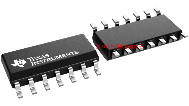
SN65MLVD207�������ͺ��У�SN65MLVD207D��SN65MLVD207DR����������Щ��Ʒ�Ĺؼ������������ɹ����ۣ�
SN65MLVD207D�������¶ȣ�-40 to 85����װ��SOIC (D)-14����װ����MPQ��50����MSL �ȼ�/��������ֵ�¶ȣ�Level-1-260C-UNLIM�����ŶƲ�/������ϣ�NIPDAU��TI����SN65MLVD207D������USD�۸�1.404��1000+��
SN65MLVD207DR�������¶ȣ�-40 to 85����װ��SOIC (D)-14����װ����MPQ��2500����MSL �ȼ�/��������ֵ�¶ȣ�Level-1-260C-UNLIM�����ŶƲ�/������ϣ�NIPDAU��TI����SN65MLVD207DR������USD�۸�1.17��1000+��

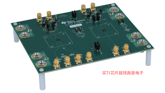
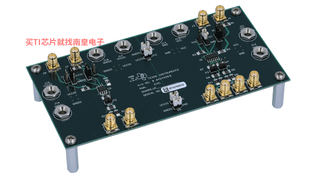
MLVD20XBEVM �� SN65MLVD203B and SN65MLVD204B full-duplex and half-duplex multipoint LVDS (M-LVDS) evaluation module
������ģ�������� M-LVDS �շ��� SN65MLVD203B �� SN65MLVD204B��SN65MLVD203B ��ȫ˫���շ�����SN65MLVD204B �ǰ�˫���շ�����
SN65MLVD207 IBIS Model
PSpice for TI ���ṩ��������ģ���·���ܵ���ƺͷ��滷�����˹�����ȫ����ƺͷ�����ʹ�� Cadence ��ģ��������档PSpice for TI �����ʹ�ã�����ҵ�ڳ����ģ�Ϳ�֮һ���������ǵ�ģ��͵�Դ��Ʒϵ���Լ���ѡ��ģ����Ϊģ�͡�����?PSpice for TI ����ƺͷ��滷���������õ�ģ�Ϳ⣬���ɶԸ��ӵĻ���ź���ƽ��з��档�����������ն��豸��ƺ�ԭ�ͽ��������Ȼ���ٽ��в��ֺ����죬�����̲�Ʒ����ʱ�䲢���Ϳ����ɱ���
��?PSpice for TI ��ƺͷ��湤���У����������� TI (...)
TINA-TI �� ���� SPICE ��ģ��������
TINA-TI �ṩ�� SPICE ���еĴ�ͳֱ����˲̬��Ƶ������Լ����ࡣTINA ���й㷺�ĺ������ܣ�����������ϣ���ķ�ʽ���ý���ĸ�ʽ����������������ѡ�����벨�Ρ�̽���·�ڵ��ѹ�Ͳ��Ρ�TINA ��ԭ��ͼ����dz�ֱ�� - �����ġ��������š���TINA-TI ��װ��Ҫ��Լ 500MB��ֱ�Ӱ�װ�������ж��Ҳ�����ס������������϶��ᰮ�����֡�
TINA �ǵ������� (TI) ר�е� DesignSoft ��Ʒ������Ѱ汾���������Ĺ��ܣ�����֧�������� TINA ���ṩ��ijЩ�������ܡ�
�����ȡ���� TINA-TI ģ�͵������б�������ģ�SpiceRack - �����б�
��Ҫ HSpice (...)


