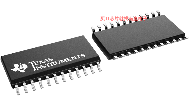
- 制造厂商:TI
- 产品类别:逻辑和电压转换
- 技术类目:缓冲器、驱动器和收发器 - 通用收发器
- 功能描述:具有三态输出的八路总线收发器和寄存器
- 点击这里打开及下载SN74ABT651的技术文档资料
- TI代理渠道,提供当日发货、严格的质量标准,满足您的目标价格

These devices consist of bus-transceiver circuits, D-type flip-flops, and control circuitry arranged for multiplexed transmission of data directly from the data bus or from the internal storage registers. Output-enable (OEAB and OEBA\) inputs are provided to control the transceiver functions. The select-control (SAB and SBA) inputs are provided to select whether real-time or stored data is transferred. A low input level selects real-time data, and a high input level selects stored data. Figure 1 illustrates the four fundamental bus-management functions that can be performed with the 'ABT651 devices.
Data on the A or B bus, or both, can be stored in the internal D flip-flops by low-to-high transitions at the appropriate clock (CLKAB or CLKBA) inputs, regardless of the select- or enable-control pins. When SAB and SBA are in the real-time transfer mode, it also is possible to store data without using the internal D-type flip-flops by simultaneously enabling OEAB and OEBA\. In this configuration, each output reinforces its input. When all the other data sources to the two sets of bus lines are at high impedance, each set remains at its last state.
To ensure the high-impedance state during power up or power down, OEBA\ should be tied to VCC through a pullup resistor; the minimum value of the resistor is determined by the current-sinking capability of the driver (B to A). OEAB should be tied to GND through a pulldown resistor; the minimum value of the resistor is determined by the current-sourcing capability of the driver (A to B).
The SN54ABT651 is characterized for operation over the full military temperature range of -55°C to 125°C. The SN74ABT651 is characterized for operation from -40°C to 85°C.
 The data output functions may be enabled or disabled by a variety of level combinations at OEAB or OEBA\. Data input functions are always enabled; i.e., data at the bus terminals is stored on every low-to-high transition of the clock inputs.
 When select control is low, clocks can occur simultaneously if allowances are made for propagation delays from A to B (B to A) plus setup and hold times. When select control is high, clocks must be staggered to load both registers.
Figure 1. Bus-Management Functions
- State-of-the-Art EPIC-II BTM BiCMOS Design Significantly Reduces Power Dissipation
- ESD Protection Exceeds 2000 V Per MIL-STD-883, Method 3015; Exceeds 200 V Using Machine Model (C = 200 pF, R = 0)
- Latch-Up Performance Exceeds 500 mA Per JESD 17
- Typical VOLP (Output Ground Bounce) < 1 V at VCC = 5 V, TA = 25°C
- High-Drive Outputs (-32-mA IOH, 64-mA IOL)
- Multiplexed Real-Time and Stored Data
- Inverting Data Paths
- Package Options Include Plastic Small-Outline (DW), Shrink Small-Outline (DB), and Thin Shrink Small-Outline (PW) Packages, Ceramic Chip Carriers (FK), and Plastic (NT) and Ceramic (JT) DIPs
EPIC-IIB is a trademark of Texas Instruments Incorporated.
- IOL (Max) (mA)
- 64
- IOH (Max) (mA)
- -32
- Technology Family
- ABT
- Rating
- Catalog
- Operating temperature range (C)
- -40 to 85
SN74ABT651的完整型号有:SN74ABT651DW、SN74ABT651DWR,以下是这些产品的关键参数及官网采购报价:
SN74ABT651DW,工作温度:-40 to 85,封装:SOIC (DW)-24,包装数量MPQ:25个,MSL 等级/回流焊峰值温度:Level-1-260C-UNLIM,引脚镀层/焊球材料:NIPDAU,TI官网SN74ABT651DW的批量USD价格:1.832(1000+)
SN74ABT651DWR,工作温度:-40 to 85,封装:SOIC (DW)-24,包装数量MPQ:2000个,MSL 等级/回流焊峰值温度:Level-1-260C-UNLIM,引脚镀层/焊球材料:NIPDAU,TI官网SN74ABT651DWR的批量USD价格:1.527(1000+)

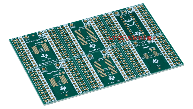
14-24-LOGIC-EVM ― 支持 14 到 24 引脚 PW、DB、D、DW、NS、DYY 和 DGV 封装的通用逻辑 EVM
该 EVM 设计用于支持采用 14 至 24 引脚 D、DW、DB、NS、PW、DYY 或 DGV 封装的任何逻辑器件。


