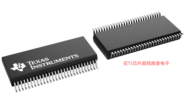
- 制造厂商:TI
- 产品类别:逻辑和电压转换
- 技术类目:缓冲器、驱动器和收发器 - 通用收发器
- 功能描述:具有奇偶校验器和双路三态输出的 3.3V 12 位通用总线驱动器
- 点击这里打开及下载SN74ALVCH16903的技术文档资料
- TI代理渠道,提供当日发货、严格的质量标准,满足您的目标价格

This 12-bit universal bus driver is designed for 2.3-V to 3.6-V VCC operation.
The SN74ALVCH16903 has dual outputs and can operate as a buffer or an edge-triggered register. In both modes, parity is checked on APAR, which arrives one cycle after the data to which it applies. The YERR\ output, which is produced one cycle after APAR, is open drain.
MODE selects one of the two data paths. When MODE is low, the device operates as an edge-triggered register. On the positive transition of the clock (CLK) input and when the clock-enable (CLKEN\) input is low, data set up at the A inputs is stored in the internal registers. On the positive transition of CLK and when CLKEN\ is high, only data set up at the 9A-12A inputs is stored in their internal registers. When MODE is high, the device operates as a buffer and data at the A inputs passes directly to the outputs. 11A/YERREN\ serves a dual purpose; it acts as a normal data bit and also enables YERR\ data to be clocked into the YERR\ output register.
When used as a single device, parity output enable (PAROE\) must be tied high; when parity input/output (PARI/O) is low, even parity is selected and when PARI/O is high, odd parity is selected. When used in pairs and PAROE\ is low, the parity sum is output on PARI/O for cascading to the second SN74ALVCH16903. When used in pairs and PAROE\ is high, PARI/O accepts a partial parity sum from the first SN74ALVCH16903.
A buffered output-enable (OE\) input can be used to place the 24 outputs and YERR\ in either a normal logic state (high or low logic levels) or a high-impedance state. In the high-impedance state, the outputs neither load nor drive the bus lines significantly. The high-impedance state and increased drive provide the capability to drive bus lines without need for interface or pullup components.
OE\ does not affect the internal operation of the device. Old data can be retained or new data can be entered while the outputs are in the high-impedance state.
To ensure the high-impedance state during power up or power down, OE\ should be tied to VCC through a pullup resistor; the minimum value of the resistor is determined by the current-sinking capability of the driver.
Active bus-hold circuitry is provided to hold unused or floating data inputs at a valid logic level.
The SN74ALVCH16903 is characterized for operation from 0°C to 70°C.
- Member of the Texas Instruments Widebus? Family
- EPIC? (Enhanced-Performance Implanted CMOS) Submicron Process
- Checks Parity
- Able to Cascade With a Second SN74ALVCH16903
- ESD Protection Exceeds 2000 V Per MIL-STD-883, Method 3015; Exceeds 200 V Using Machine Model (C = 200 pF, R = 0)
- Latch-Up Performance Exceeds 250 mA Per JESD 17
- Bus Hold on Data Inputs Eliminates the Need for External Pullup/Pulldown Resistors
- Package Options Include Plastic 300-mil Shrink Small-Outline (DL), Thin Shrink Small-Outline (DGG), and Thin Very Small-Outline (DGV) Packages
Widebus, EPIC are trademarks of Texas Instruments.
- IOL (Max) (mA)
- 24
- IOH (Max) (mA)
- -32
- Technology Family
- ALVC
- Rating
- Catalog
- Operating temperature range (C)
- -40 to 85
SN74ALVCH16903的完整型号有:SN74ALVCH16903DL,以下是这些产品的关键参数及官网采购报价:
SN74ALVCH16903DL,工作温度:-40 to 85,封装:SSOP (DL)-56,包装数量MPQ:20个,MSL 等级/回流焊峰值温度:Level-1-260C-UNLIM,引脚镀层/焊球材料:NIPDAU,TI官网SN74ALVCH16903DL的批量USD价格:6.321(1000+)

SN74ALVCH16903DL,工作温度:-40 to 85,封装:SSOP (DL)-56,包装数量MPQ:20个,MSL 等级/回流焊峰值温度:Level-1-260C-UNLIM,引脚镀层/焊球材料:NIPDAU,TI官网SN74ALVCH16903DL的批量USD价格:6.321(1000+)


