- 制造厂商:TI
- 产品类别:逻辑和电压转换
- 技术类目:专用逻辑 IC - 数字算术 IC
- 功能描述:八路幅度比较器
- 点击这里打开及下载SN74AS885的技术文档资料
- TI代理渠道,提供当日发货、严格的质量标准,满足您的目标价格

These advanced Schottky devices are capable of performing high-speed arithmetic or logic comparisons on two 8-bit binary or two's complement words. Two fully decoded decisions about words P and Q are externally available at two outputs. These devices are fully expandable to any number of bits without external gates. To compare words of longer lengths, the P > QOUT and P < QOUT outputs of a stage handling less significant bits can be connected to the P > QIN and P < QIN inputs of the next stage handling more significant bits. The cascading paths are implemented with only a two-gate-level delay to reduce overall comparison times for long words. Two alternative methods of cascading are shown in application information.
The latch is transparent when P latch-enable (PLE) input is high; the P-input port is latched
when PLE is low. This provides the designer with temporary storage for the P-data word. The enable circuitry is implemented with minimal delay times to enhance performance when cascaded for longer words. The PLE, P, and Q data inputs utilize pnp input transistors to reduce the low-level current input requirement to typically -0.25 mA, which minimizes dc loading effects.
The SN54AS885 is characterized for operation over the full military temperature range of -55°C to 125°C. The SN74AS885 is characterized for operation from 0°C to 70°C.
In these cases, P > QOUT follows P > QIN and P < QOUT follows P < QIN.
AG = arithmetically greater than
- Latchable P-Input Ports With Power-Up Clear
- Choice of Logical or Arithmetic (Two's Complement) Comparison
- Data and PLE Inputs Utilize pnp Input Transistors to Reduce dc Loading Effects
- Approximately 35% Improvement in ac Performance Over Schottky TTL While Performing More Functions
- Cascadable to n Bits While Maintaining High Performance
- 10% Less Power Than STTL for an 8-Bit Comparison
- Package Options Include Plastic Small-Outline (DW) Packages, Ceramic Chip Carriers (FK), and Standard Plastic (NT) and Ceramic (JT) 300-mil DIPs
- Number of channels (#)
- 8
- Technology Family
- AS
- Input type
- Bipolar
- Output type
- Push-Pull
- Features
- High speed (tpd 10-50ns)
SN74AS885的完整型号有:SN74AS885DW,以下是这些产品的关键参数及官网采购报价:
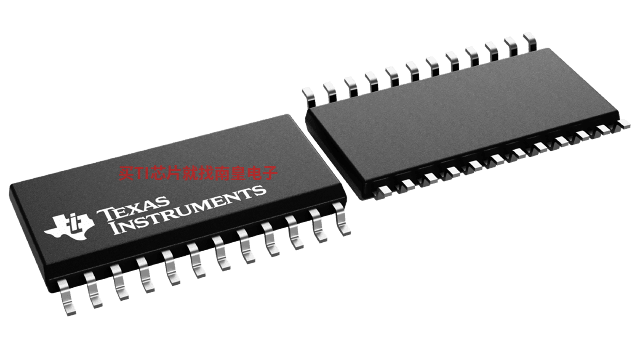
SN74AS885DW,工作温度:0 to 70,封装:SOIC (DW)-24,包装数量MPQ:25个,MSL 等级/回流焊峰值温度:Level-1-260C-UNLIM,引脚镀层/焊球材料:NIPDAU,TI官网SN74AS885DW的批量USD价格:7.893(1000+)

14-24-LOGIC-EVM ― 支持 14 到 24 引脚 PW、DB、D、DW、NS、DYY 和 DGV 封装的通用逻辑 EVM
该 EVM 设计用于支持采用 14 至 24 引脚 D、DW、DB、NS、PW、DYY 或 DGV 封装的任何逻辑器件。