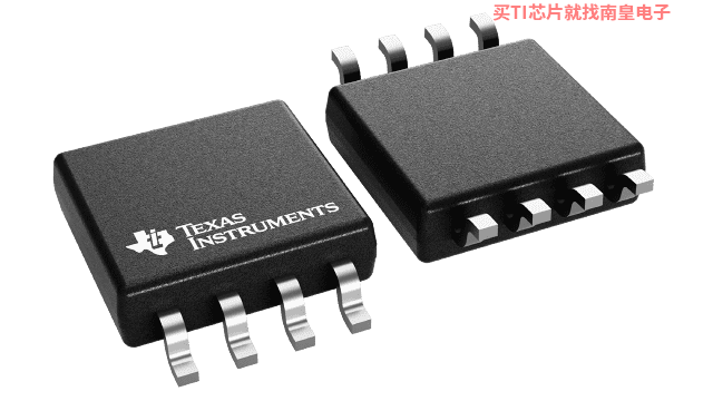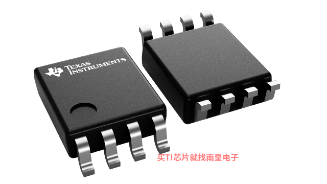
- 制造厂商:TI
- 产品类别:逻辑和电压转换
- 技术类目:缓冲器、驱动器和收发器 - 同相缓冲器和驱动器
- 功能描述:具有三态输出的 2 通道、0.8V 至 2.7V 高速缓冲器
- 点击这里打开及下载SN74AUC2G241的技术文档资料
- TI代理渠道,提供当日发货、严格的质量标准,满足您的目标价格

This dual buffer/driver is operational at 0.8-V to 2.7-V VCC, but is designed specifically for 1.65-V to 1.95-V VCC operation.
The SN74AUC2G241 is designed specifically to improve the performance and density of 3-state memory address drivers, clock drivers, and bus-oriented receivers and transmitters.
The device is organized as two 1-bit line drivers with separate output-enable (1OE, 2OE) inputs. When 1OE is low or 2OE is high, the device passes data from the A inputs to the Y outputs. When 1OE is high or 2OE is low, the outputs are in the high-impedance state.
NanoFree™ package technology is a major breakthrough in IC packaging concepts, using the die as the package.
To ensure the high-impedance state during power up or power down, OE should be tied to VCC through a pullup resistor, and OE should be tied to GND through a pulldown resistor; the minimum value of the resistor is determined by the current-sinking/current-sourcing capability of the driver.
This device is fully specified for partial-power-down applications using Ioff. The Ioff circuitry disables the outputs, preventing damaging current backflow through the device when it is powered down.
For more information about AUC Little Logic devices, please refer to the TI application report, Applications of Texas Instruments AUC Sub-1-V Little Logic Devices, literature number SCEA027.
- Available in the Texas Instruments NanoFree? Package
- Optimized for 1.8-V Operation and Is 3.6-V I/O Tolerant to Support Mixed-Mode Signal Operation
- Ioff Supports Partial-Power-Down Mode Operation
- Sub-1-V Operable
- Max tpd of 1.9 ns at 1.8 V
- Low Power Consumption, 10 μA at 1.8 V
- ±8-mA Output Drive at 1.8 V
- Latch-Up Performance Exceeds 100 mA Per JESD 78, Class II
- ESD Protection Exceeds JESD 22
- 2000-V Human-Body Model (A114-A)
- 200-V Machine Model (A115-A)
- 1000-V Charged-Device Model (C101)
NanoFree is a trademark of Texas Instruments.
- Technology Family
- AUC
- Supply voltage (Min) (V)
- 0.8
- Supply voltage (Max) (V)
- 2.7
- Number of channels (#)
- 2
- IOL (Max) (mA)
- 9
- ICC (Max) (uA)
- 10
- IOH (Max) (mA)
- -9
- Input type
- Standard CMOS
- Output type
- 3-State
- Features
- Balanced outputs, Ultra high speed (tpd <5ns), Partial power down (Ioff), Over-voltage tolerant inputs
- Rating
- Catalog
SN74AUC2G241的完整型号有:SN74AUC2G241DCTR、SN74AUC2G241DCUR、SN74AUC2G241YZPR,以下是这些产品的关键参数及官网采购报价:
SN74AUC2G241DCTR,工作温度:-40 to 85,封装:SM8 (DCT)-8,包装数量MPQ:3000个,MSL 等级/回流焊峰值温度:Level-1-260C-UNLIM,引脚镀层/焊球材料:NIPDAU,TI官网SN74AUC2G241DCTR的批量USD价格:.249(1000+)
SN74AUC2G241DCUR,工作温度:-40 to 85,封装:VSSOP (DCU)-8,包装数量MPQ:3000个,MSL 等级/回流焊峰值温度:Level-1-260C-UNLIM,引脚镀层/焊球材料:NIPDAU,TI官网SN74AUC2G241DCUR的批量USD价格:.189(1000+)
SN74AUC2G241YZPR,工作温度:-40 to 85,封装:DSBGA (YZP)-8,包装数量MPQ:3000个,MSL 等级/回流焊峰值温度:Level-1-260C-UNLIM,引脚镀层/焊球材料:SNAGCU,TI官网SN74AUC2G241YZPR的批量USD价格:.249(1000+)

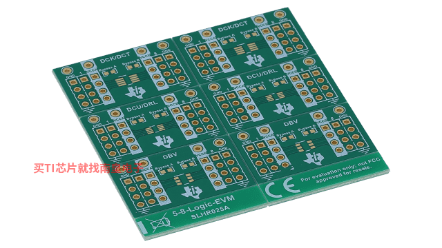
5-8-LOGIC-EVM ― 支持 5 至 8 引脚 DCK、DCT、DCU、DRL 和 DBV 封装的通用逻辑 EVM
灵活的 EVM 设计用于支持具有 5 至 8 引脚数且采用 DCK、DCT、DCU、DRL 或 DBV 封装的任何器件。


