- жЦдьГЇЩЬЃКTI
- ВњЦЗРрБ№ЃКТпМКЭЕчбЙзЊЛЛ
- ММЪѕРрФПЃКТпМУХ - ЕчбЙзЊЛЛУХ
- ЙІФмУшЪіЃКЕЭЙІКФЁЂ1.8/2.5/3.3V ЪфШыЁЂ3.3V CMOS ЪфГіЁЂЕЅТЗ 2 ЪфШые§ЛђЗЧУХ
- ЕуЛїетРяДђПЊМАЯТдиSN74AUP1T02ЕФММЪѕЮФЕЕзЪСЯ
- TIДњРэЧўЕРЃЌЬсЙЉЕБШеЗЂЛѕЁЂбЯИёЕФжЪСПБъзМЃЌТњзуФњЕФФПБъМлИё

The SN74AUP1T02 performs the Boolean function Y = A + B or Y = A • B with designation for logic-level translation applications with output referenced to supply VCC.
AUP technology is the industry’s lowest-power logic technology designed for use in extending battery-life in operating. All input levels that accept 1.8-V LVCMOS signals, while operating from either a single 3.3-V or 2.5-V VCC supply. This product also maintains excellent signal integrity (see Figure 1 and Figure 2).
The wide VCC range of 2.3 V to 3.6 V allows the possibility of switching output level to connect to external controllers or processors.
Schmitt-trigger inputs ( VT = 210 mV between positive and negative input transitions) offer improved noise immunity during switching transitions, which is especially useful on analog mixed-mode designs. Schmitt-trigger inputs reject input noise, ensure integrity of output signals, and allow for slow input signal transition.
Ioff is a feature that allows for powered-down conditions (VCC = 0 V) and is important in portable and mobile applications. When VCC = 0 V, signals in the range from 0 V to 3.6 V can be applied to the inputs and outputs of the device. No damage occurs to the device under these conditions.
The SN74AUP1T02 is designed with optimized current-drive capability of 4 mA to reduce line reflections, overshoot, and undershoot caused by high-drive outputs.
- Single-Supply Voltage Translator
- Output Level Up to Supply VCC CMOS Level
- 1.8 V to 3.3 V (at VCC = 3.3 V)
- 2.5 V to 3.3 V (at VCC = 3.3 V)
- 1.8 V to 2.5 V (at VCC = 2.5 V)
- 3.3 V to 2.5 V (at VCC = 2.5 V
- Schmitt-Trigger Inputs Reject Input Noise and Provide Better Output Signal Integrity
- Ioff Supports Partial Power Down (VCC = 0 V)
- Very Low Static Power Consumption: 0.1 ІЬA
- Very Low Dynamic Power Consumption: 0.9 ІЬA
- Latch-Up Performance Exceeds 100 mA Per JESD 78, Class II
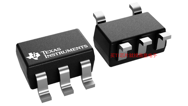
- Pb-Free Packages Available: SC-70 (DCK) 2 x 2.1 x 0.65 mm (Height 1.1 mm)
- More Gate Options Available at www.ti.com/littlelogic
- ESD Performance Tested Per JESD 22
- 2000-V Human-Body Model (A114-B, Class II)
- 1000-V Charged-Device Model (C101)
- Technology Family
- AUP1T
- Bits (#)
- 1
- High input voltage (Min) (Vih)
- 1.35
- High input voltage (Max) (Vih)
- 3.6
- Vout (Min) (V)
- 2.3
- Vout (Max) (V)
- 3.6
- IOH (Max) (mA)
- -4
- IOL (Max) (mA)
- 4
SN74AUP1T02ЕФЭъећаЭКХгаЃКSN74AUP1T02DCKRЃЌвдЯТЪЧетаЉВњЦЗЕФЙиМќВЮЪ§МАЙйЭјВЩЙКБЈМлЃК
SN74AUP1T02DCKRЃЌЙЄзїЮТЖШЃК-40 to 85ЃЌЗтзАЃКSC70 (DCK)-5ЃЌАќзАЪ§СПMPQЃК3000ИіЃЌMSL ЕШМЖ/ЛиСїКИЗхжЕЮТЖШЃКLevel-1-260C-UNLIMЃЌв§НХЖЦВу/КИЧђВФСЯЃКNIPDAUЃЌTIЙйЭјSN74AUP1T02DCKRЕФХњСПUSDМлИёЃК.059ЃЈ1000+ЃЉ

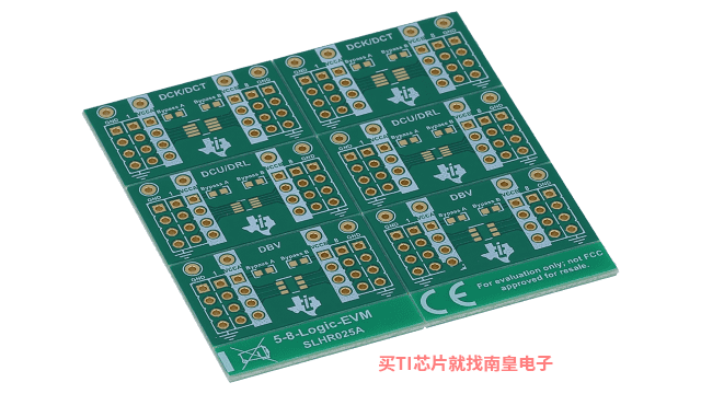
5-8-LOGIC-EVM ЁЊ жЇГж 5 жС 8 в§НХ DCKЁЂDCTЁЂDCUЁЂDRL КЭ DBV ЗтзАЕФЭЈгУТпМ EVM
СщЛюЕФ EVM ЩшМЦгУгкжЇГжОпга 5 жС 8 в§НХЪ§ЧвВЩгУ DCKЁЂDCTЁЂDCUЁЂDRL Лђ DBV ЗтзАЕФШЮКЮЦїМўЁЃ


