- 制造厂商:TI
- 产品类别:逻辑和电压转换
- 技术类目:逻辑门 - 电压转换门
- 功能描述:低功耗、1.8/2.5/3.3V 输入、3.3V CMOS 输出、缓冲多路复用器(同向)
- 点击这里打开及下载SN74AUP1T157的技术文档资料
- TI代理渠道,提供当日发货、严格的质量标准,满足您的目标价格

The SN74AUP1T157 is a single 2-input multiplexer that selects data from two data inputs (A and B) under control of a common data select input (C). The state of the common data select input determines the particular register from which the data comes. The output (Y) presents the selected data in the true (non-inverted) form.
AUP technology is the industry’s lowest-power logic technology designed for use in extending battery-life in operating. All input levels that accept 1.8-V LVCMOS signals, while operating from either a single 3.3-V or 2.5-V VCC supply. This product also maintains excellent signal integrity (see Figure 2 and Figure 3).
The wide VCC range of 2.3 V to 3.6 V allows the possibility of switching output level to connect to external controllers or processors.
Schmitt-trigger inputs ( VT = 210 mV between positive and negative input transitions) offer improved noise immunity during switching transitions, which is especially useful on analog mixed-mode designs. Schmitt-trigger inputs reject input noise, ensure integrity of output signals, and allow for slow input signal transition.
Ioff is a feature that allows for powered-down conditions (VCC = 0 V) and is important in portable and mobile applications. When VCC = 0 V, signals in the range from 0 V to 3.6 V can be applied to the inputs and outputs of the device. No damage occurs to the device under these conditions.
The SN74AUP1T157 is designed with optimized current-drive capability of 4 mA to reduce line reflections, overshoot, and undershoot caused by high-drive outputs.
- Single-Supply Voltage Translator
- Output Level Up to Supply VCC CMOS Level
- 1.8 V to 3.3 V (at VCC = 3.3 V)
- 2.5 V to 3.3 V (at VCC = 3.3 V)
- 1.8 V to 2.5 V (at VCC = 2.5 V)
- 3.3 V to 2.5 V (at VCC = 2.5 V
- Schmitt-Trigger Inputs Reject Input Noise and Provide Better Output Signal Integrity
- Ioff Supports Partial Power Down (VCC = 0 V)
- Very Low Static Power Consumption: 0.1 μA
- Very Low Dynamic Power Consumption: 0.9 μA
- Latch-Up Performance Exceeds 100 mA Per JESD 78, Class II
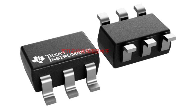
- Pb-Free Packages Available: SC-70 (DCK) 2 x 2.1 x 0.65 mm (Height 1.1 mm)
- More Gate Options Available at www.ti.com/littlelogic
- ESD Performance Tested Per JESD 22
- 2000-V Human-Body Model (A114-B, Class II)
- 1000-V Charged-Device Model (C101)
- Technology Family
- AUP1T
- Bits (#)
- 1
- High input voltage (Min) (Vih)
- 1.35
- High input voltage (Max) (Vih)
- 3.6
- Vout (Min) (V)
- 2.3
- Vout (Max) (V)
- 3.6
- IOH (Max) (mA)
- -4
- IOL (Max) (mA)
- 4
SN74AUP1T157的完整型号有:SN74AUP1T157DCKR,以下是这些产品的关键参数及官网采购报价:
SN74AUP1T157DCKR,工作温度:-40 to 85,封装:SC70 (DCK)-6,包装数量MPQ:3000个,MSL 等级/回流焊峰值温度:Level-1-260C-UNLIM,引脚镀层/焊球材料:NIPDAU,TI官网SN74AUP1T157DCKR的批量USD价格:0.073(1000+)

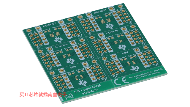
5-8-LOGIC-EVM ― 支持 5 至 8 引脚 DCK、DCT、DCU、DRL 和 DBV 封装的通用逻辑 EVM
灵活的 EVM 设计用于支持具有 5 至 8 引脚数且采用 DCK、DCT、DCU、DRL 或 DBV 封装的任何器件。