- 制造厂商:TI
- 产品类别:逻辑和电压转换
- 技术类目:电压转换器和电平转换器 - 固定方向电压转换器
- 功能描述:低功耗、1.8/2.5/3.3V 输入、3.3V CMOS 输出、单路施密特触发缓冲门
- 点击这里打开及下载SN74AUP1T17的技术文档资料
- TI代理渠道,提供当日发货、严格的质量标准,满足您的目标价格

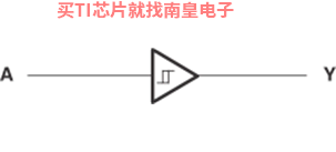
The SN74AUP1T17 performs the Boolean function Y = A with designation for logic-level translation applications with output referenced to supply VCC.
AUP technology is the industry–s lowest-power logic technology designed for use in extending battery-life in operating. All input levels that accept 1.8-V LVCMOS signals, while operating from either a single 3.3-V or 2.5-V VCC supply. This product also maintains excellent signal integrity.
The wide VCC range of 2.3 V to 3.6 V allows the possibility of switching output level to connect to external controllers or processors.
Schmitt-trigger inputs (ΔVT = 210 mV between positive and negative input transitions) offer improved noise immunity during switching transitions, which is especially useful on analog mixed-mode designs. Schmitt-trigger inputs reject input noise, ensure integrity of output signals, and allow for slow input signal transition.
Ioff is a feature that allows for powered-down conditions (VCC = 0 V) and is important in portable and mobile applications. When VCC = 0 V, signals in the range from 0 V to 3.6 V can be applied to the inputs and outputs of the device. No damage occurs to the device under these conditions.
The SN74AUP1T17 is designed with optimized current-drive capability of 4 mA to reduce line reflections, overshoot, and undershoot caused by high-drive outputs.
- Single-Supply Voltage Translator
- Output Level Up to Supply VCC CMOS Level
- 1.8 V to 3.3 V (at VCC = 3.3 V)
- 2.5 V to 3.3 V (at VCC = 3.3 V)
- 1.8 V to 2.5 V (at VCC = 2.5 V)
- 3.3 V to 2.5 V (at VCC = 2.5 V
- Schmitt-Trigger Inputs Reject Input Noise and Provide Better Output Signal Integrity
- Ioff Supports Partial Power Down (VCC = 0 V)
- Very Low Static Power Consumption: 0.1 μA
- Very Low Dynamic Power Consumption: 0.9 μA
- Latch-Up Performance Exceeds 100 mA Per JESD 78, Class II
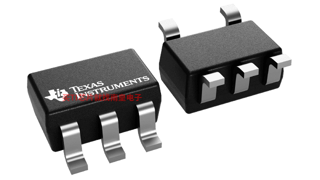
- Pb-Free Packages Available: SC-70 (DCK) 2 × 2.1 × 0.65 mm (Height 1.1 mm)
- More Gate Options Available at www.ti.com/littlelogic
- ESD Performance Tested Per JESD 22
- 2000-V Human Body Model (A114-B, Class II)
- 1000-V Charged-Device Model (C101)
- APPLICATIONS
- AV Receivers
- Audio Dock: Portable
- Blu-ray Players and Home Theaters
- MP3 Players and Recorders
- Personal Digital Assistant (PDA)
- Power: Telecom/Server AC/DC Supply: Single Controller: Analog and Digital
- Solid State Drive (SSD): Client and Enterprise
- TV: LCD/Digital and High-Definition (HDTV)
- Tablet: Enterprise
- Video Analytics: Servers
- Wireless Headsets, Keyboards, and Mice
All other trademarks are the property of their respective owners
- Technology Family
- AUP1T
- Bits (#)
- 1
- Configuration
- 1 Ch A to B; 0 Ch B to A
- Vout (Min) (V)
- 2.3
- Vout (Max) (V)
- 3.6
- IOH (Max) (mA)
- -4
- IOL (Max) (mA)
- 4
- Rating
- Catalog
SN74AUP1T17的完整型号有:SN74AUP1T17DCKR,以下是这些产品的关键参数及官网采购报价:
SN74AUP1T17DCKR,工作温度:-40 to 85,封装:SC70 (DCK)-5,包装数量MPQ:3000个,MSL 等级/回流焊峰值温度:Level-1-260C-UNLIM,引脚镀层/焊球材料:NIPDAU,TI官网SN74AUP1T17DCKR的批量USD价格:.158(1000+)

5-8-LOGIC-EVM ― 支持 5 至 8 引脚 DCK、DCT、DCU、DRL 和 DBV 封装的通用逻辑 EVM
灵活的 EVM 设计用于支持具有 5 至 8 引脚数且采用 DCK、DCT、DCU、DRL 或 DBV 封装的任何器件。TIDA-00268 ― Thunderbolt™ 单端口外设参考设计
TI Thunderbolt 单端口外设参考设计已针对具有 20Gbps 带宽的 Thunderbolt 2 系统进行优化。此设计利用 TPS65980 电源管理单元,与离散式实施相比,可将 BOM 成本降低达 50%,将面积降低约 40%。此设计已在 Intel 针对自供电和总线供电的单端口 Thunderbolt 系统进行测试和认证。