- ���쳧�̣�TI
- ��Ʒ������͵�ѹת��
- ������Ŀ�������������������շ��� - ͬ�������������
- ����������������̬����� 2 ͨ����0.8V �� 3.6V ���Ļ�����
- ������������SN74AUP2G125�ļ����ĵ�����
- TI�����������ṩ���շ������ϸ������������������Ŀ��۸�

The AUP family is TI’s premier solution to the industry’s low-power needs in battery-powered portable applications. This family ensures a very low static and dynamic power consumption across the entire VCC range of 0.8 V to 3.6 V, resulting in an increased battery life. This product also maintains excellent signal integrity (see Figure 1 and Figure 2).
The SN74AUP2G125 is a dual bus buffer gate designed for 0.8-V to 3.6-V VCC operation. This device features dual line drivers with 3-state outputs. Each output is disabled when the corresponding output-enable (OE) input is high. This device has the input-disable feature, which allows floating input signals.
To ensure the high-impedance state during power up or power down, OE should be tied to VCC through a pullup resistor; the minimum value of the resistor is determined by the current-sinking capability of the driver.
NanoStar™ package technology is a major breakthrough in IC packaging concepts, using the die as the package.
This device is fully specified for partial-power-down applications using Ioff. The Ioff circuitry disables the outputs, preventing damaging current backflow through the device when it is powered down.
- Available in the Texas Instruments NanoStar? Package
- Low Static-Power Consumption (ICC = 0.9 ��A Max)
- Low Dynamic-Power Consumption (Cpd = 4 pF Typ at 3.3 V)
- Low Input Capacitance (CI = 1.5 pF Typ)
- Low Noise �C Overshoot and Undershoot <10% of VCC
- Input-Disable Feature Allows Floating Input Conditions
- Ioff Supports Partial-Power-Down Mode Operation
- Input Hysteresis Allows Slow Input Transition and Better Switching Noise Immunity at Input
- Wide Operating VCC Range of 0.8 V to 3.6 V
- Optimized for 3.3-V Operation
- 3.6-V I/O Tolerant to Support Mixed-Mode Signal Operation
- tpd = 5.4 ns Max at 3.3 V
- Suitable for Point-to-Point Applications
- Latch-Up Performance Exceeds 100 mA Per JESD 78, Class II
- ESD Performance Tested Per JESD 22
- 2000-V Human-Body Model (A114-B, Class II)
- 1000-V Charged-Device Model (C101)
NanoStar is a trademark of Texas Instruments
- Technology Family
- AUP
- Supply voltage (Min) (V)
- 0.8
- Supply voltage (Max) (V)
- 3.6
- Number of channels (#)
- 2
- IOL (Max) (mA)
- 4
- ICC (Max) (uA)
- 0.9
- IOH (Max) (mA)
- -4
- Input type
- Standard CMOS
- Output type
- 3-State
- Features
- Balanced outputs, Very high speed (tpd 5-10ns), Partial power down (Ioff), Over-voltage tolerant inputs
- Rating
- Catalog
SN74AUP2G125�������ͺ��У�SN74AUP2G125DCUR��SN74AUP2G125DQER��SN74AUP2G125RSER��SN74AUP2G125YFPR��SN74AUP2G125YZPR����������Щ��Ʒ�Ĺؼ������������ɹ����ۣ�
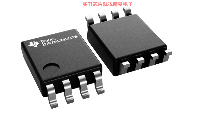
SN74AUP2G125DCUR�������¶ȣ�-40 to 85����װ��VSSOP (DCU)-8����װ����MPQ��3000����MSL �ȼ�/��������ֵ�¶ȣ�Level-1-260C-UNLIM�����ŶƲ�/������ϣ�NIPDAU��TI����SN74AUP2G125DCUR������USD�۸�.189��1000+��
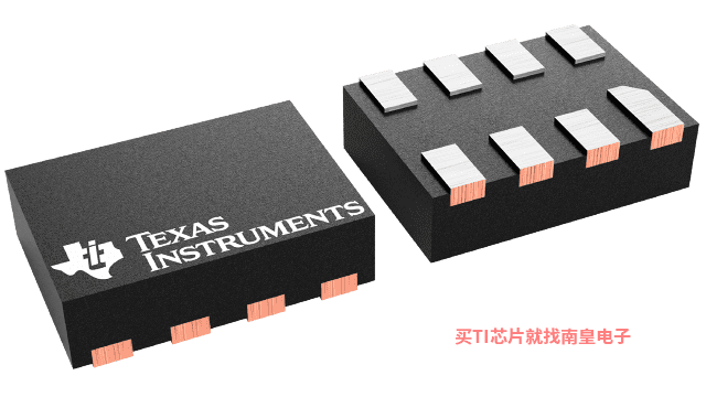
SN74AUP2G125DQER�������¶ȣ�-40 to 85����װ��X2SON (DQE)-8����װ����MPQ��5000����MSL �ȼ�/��������ֵ�¶ȣ�Level-1-260C-UNLIM�����ŶƲ�/������ϣ�NIPDAUAG��TI����SN74AUP2G125DQER������USD�۸�.198��1000+��
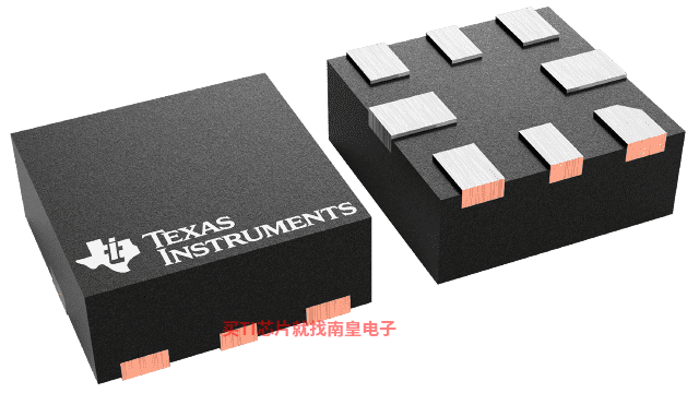
SN74AUP2G125RSER�������¶ȣ�-40 to 85����װ��UQFN (RSE)-8����װ����MPQ��5000����MSL �ȼ�/��������ֵ�¶ȣ�Level-1-260C-UNLIM�����ŶƲ�/������ϣ�NIPDAUAG��TI����SN74AUP2G125RSER������USD�۸�.246��1000+��
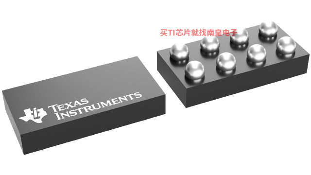
SN74AUP2G125YFPR�������¶ȣ�-40 to 85����װ��DSBGA (YFP)-8����װ����MPQ��3000����MSL �ȼ�/��������ֵ�¶ȣ�Level-1-260C-UNLIM�����ŶƲ�/������ϣ�SNAGCU��TI����SN74AUP2G125YFPR������USD�۸�.239��1000+��
SN74AUP2G125YZPR�������¶ȣ�-40 to 85����װ��DSBGA (YZP)-8����װ����MPQ��3000����MSL �ȼ�/��������ֵ�¶ȣ�Level-1-260C-UNLIM�����ŶƲ�/������ϣ�SNAGCU��TI����SN74AUP2G125YZPR������USD�۸�.249��1000+��

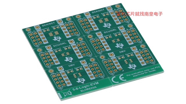
5-8-LOGIC-EVM �� ֧�� 5 �� 8 ���� DCK��DCT��DCU��DRL �� DBV ��װ��ͨ���� EVM
���� EVM �������֧�־��� 5 �� 8 �������Ҳ��� DCK��DCT��DCU��DRL �� DBV ��װ���κ�������