- 制造厂商:TI
- 产品类别:逻辑和电压转换
- 技术类目:触发器、锁存器和寄存器 - D 型触发器
- 功能描述:低功耗双路正边沿触发式 D 型触发器
- 点击这里打开及下载SN74AUP2G80的技术文档资料
- TI代理渠道,提供当日发货、严格的质量标准,满足您的目标价格

The AUP family is TI’s premier solution to the industry’s low-power needs in battery-powered portable applications. This family ensures a very low static- and dynamic-power consumption across the entire VCC range of 0.8 V to 3.6 V, resulting in increased battery life (see Figure 1). This product also maintains excellent signal integrity (see the very low undershoot and overshoot characteristics shown in Figure 2).
When data at the data (D) input meets the setup time requirement, the data is transferred to the Q output on the positive-going edge of the clock pulse. Clock triggering occurs at a voltage level and is not directly related to the rise time of the clock pulse. Following the hold-time interval, data at the D input can be changed without affecting the levels at the outputs.
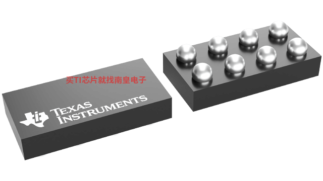
NanoStar™ package technology is a major breakthrough in IC packaging concepts, using the die as the package.
This device is fully specified for partial-power-down applications using Ioff. The Ioff circuitry disables the outputs, preventing damaging current backflow through the device when it is powered down.
- Available in the Texas Instruments NanoStar? Package
- Low Static-Power Consumption (ICC = 0.9 μA Maximum)
- Low Dynamic-Power Consumption (Cpd = 4.3 pF Typ at 3.3 V)
- Low Input Capacitance (Ci = 1.5 pF Typical)
- Low Noise – Overshoot and Undershoot <10% of VCC
- Ioff Supports Partial-Power-Down Mode Operation
- Wide Operating VCC Range of 0.8 V to 3.6 V
- Optimized for 3.3-V Operation
- 3.6-V I/O Tolerant to Support Mixed-Mode Signal Operation
- tpd = 4.4 ns Maximum at 3.3 V
- Suitable for Point-to-Point Applications
- Latch-Up Performance Exceeds 100 mA Per JESD 78, Class II
- ESD Performance Tested Per JESD 22
- 2000-V Human-Body Model (A114-B, Class II)
- 1000-V Charged-Device Model (C101)
- Number of channels (#)
- 2
- Technology Family
- AUP
- Supply voltage (Min) (V)
- 0.8
- Supply voltage (Max) (V)
- 3.6
- Input type
- Standard CMOS
- Output type
- Push-Pull
- Clock Frequency (Max) (MHz)
- 260
- IOL (Max) (mA)
- 4
- IOH (Max) (mA)
- -4
- ICC (Max) (uA)
- 0.9
- Features
- Balanced outputs, Very high speed (tpd 5-10ns), Over-voltage tolerant inputs, Partial power down (Ioff)
SN74AUP2G80的完整型号有:SN74AUP2G80DCUR、SN74AUP2G80DQER、SN74AUP2G80RSER、SN74AUP2G80YFPR,以下是这些产品的关键参数及官网采购报价:
SN74AUP2G80DCUR,工作温度:-40 to 85,封装:VSSOP (DCU)-8,包装数量MPQ:3000个,MSL 等级/回流焊峰值温度:Level-1-260C-UNLIM,引脚镀层/焊球材料:NIPDAU,TI官网SN74AUP2G80DCUR的批量USD价格:.189(1000+)
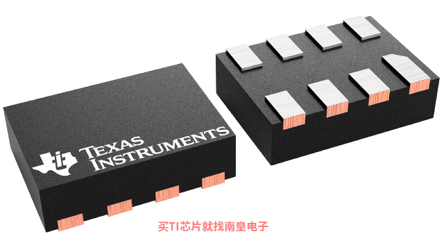
SN74AUP2G80DQER,工作温度:-40 to 85,封装:X2SON (DQE)-8,包装数量MPQ:5000个,MSL 等级/回流焊峰值温度:Level-1-260C-UNLIM,引脚镀层/焊球材料:NIPDAUAG,TI官网SN74AUP2G80DQER的批量USD价格:.198(1000+)
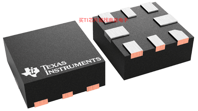
SN74AUP2G80RSER,工作温度:-40 to 85,封装:UQFN (RSE)-8,包装数量MPQ:5000个,MSL 等级/回流焊峰值温度:Level-1-260C-UNLIM,引脚镀层/焊球材料:NIPDAUAG,TI官网SN74AUP2G80RSER的批量USD价格:.246(1000+)
SN74AUP2G80YFPR,工作温度:-40 to 85,封装:DSBGA (YFP)-8,包装数量MPQ:3000个,MSL 等级/回流焊峰值温度:Level-1-260C-UNLIM,引脚镀层/焊球材料:SNAGCU,TI官网SN74AUP2G80YFPR的批量USD价格:.239(1000+)

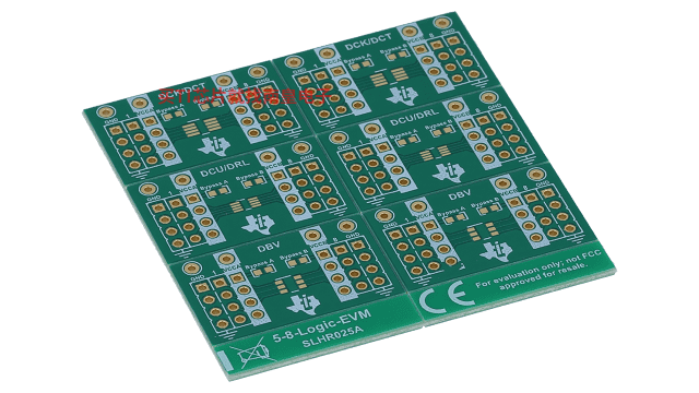
5-8-LOGIC-EVM — 支持 5 至 8 引脚 DCK、DCT、DCU、DRL 和 DBV 封装的通用逻辑 EVM
灵活的 EVM 设计用于支持具有 5 至 8 引脚数且采用 DCK、DCT、DCU、DRL 或 DBV 封装的任何器件。


