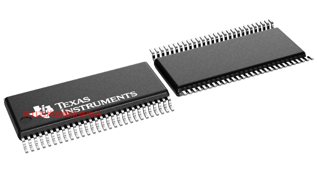
- 制造厂商:TI
- 产品类别:逻辑和电压转换
- 技术类目:缓冲器、驱动器和收发器 - 通用收发器
- 功能描述:具有三态输出的 16 位总线收发器和寄存器
- 点击这里打开及下载SN74AVC16646的技术文档资料
- TI代理渠道,提供当日发货、严格的质量标准,满足您的目标价格

A Dynamic Output Control (DOC) circuit is implemented, which, during the transition, initially lowers the output impedance to effectively drive the load and, subsequently, raises the impedance to reduce noise. Figure 1 shows typical VOL vs IOL and VOH vs IOH curves to illustrate the output impedance and drive capability of the circuit. At the beginning of the signal transition, the DOC circuit provides a maximum dynamic drive that is equivalent to a high-drive standard-output device. For more information, refer to the TI application reports, AVC Logic Family Technology and Applications, literature number SCEA006, and Dynamic Output Control (DOCTM) Circuitry Technology and Applications, literature number SCEA009.
This 16-bit bus transceiver and register is operational at 1.2-V to 3.6-V VCC, but is designed specifically for 1.65-V to 3.6-V VCC operation.
The SN74AVC16646 can be used as two 8-bit transceivers or one 16-bit transceiver. Data on the A or B bus is clocked into the registers on the low-to-high transition of the appropriate clock (CLKAB or CLKBA) input. Figure 2 illustrates the four fundamental bus-management functions that can be performed with the SN74AVC16646.
Output-enable (OE\) and direction-control (DIR) inputs are provided to control the transceiver functions. In the transceiver mode, data present at the high-impedance port may be stored in either register or in both. The select-control (SAB and SBA) inputs can multiplex stored and real-time (transparent mode) data.
The circuitry used for select control eliminates the typical decoding glitch that occurs in a multiplexer during the transition between stored and real-time data. DIR determines which bus receives data when OE\ is low. In the isolation mode (OE\ high), A data may be stored in one register and/or B data may be stored in the other register.
When an output function is disabled, the input function is still enabled and may be used to store and transmit data. Only one of the two buses, A or B, can be driven at a time.
To ensure the high-impedance state during power up or power down, OE\ should be tied to VCC through a pullup resistor; the minimum value of the resistor is determined by the current-sinking capability of the driver.
This device is fully specified for partial-power-down applications using Ioff. The Ioff circuitry disables the outputs, preventing damaging current backflow through the device when it is powered down.
The SN74AVC16646 is characterized for operation from -40°C to 85°C.
- Member of the Texas Instruments WidebusTM Family
- EPICTM (Enhanced-Performance Implanted CMOS) Submicron Process
- DOCTM (Dynamic Output Control) Circuit Dynamically Changes Output Impedance, Resulting in Noise Reduction Without Speed Degradation
- Dynamic Drive Capability Is Equivalent to Standard Outputs With IOH and IOL of ±24 mA at 2.5-V VCC
- Overvoltage-Tolerant Inputs/Outputs Allow Mixed-Voltage-Mode Data Communications
- Ioff Supports Partial-Power-Down Mode Operation
- Latch-Up Performance Exceeds 100 mA Per JESD 78, Class II
- Package Options Include Plastic Thin Shrink Small-Outline (DGG) and Thin Very Small-Outline (DGV) Packages
DOC, EPIC, and Widebus are trademarks of Texas Instruments.
- IOL (Max) (mA)
- 12
- IOH (Max) (mA)
- -12
- Technology Family
- AVC
- Rating
- Catalog
- Operating temperature range (C)
- -40 to 85
SN74AVC16646的完整型号有:SN74AVC16646DGVR,以下是这些产品的关键参数及官网采购报价:
SN74AVC16646DGVR,工作温度:-40 to 85,封装:TVSOP (DGV)-56,包装数量MPQ:2000个,MSL 等级/回流焊峰值温度:Level-1-260C-UNLIM,引脚镀层/焊球材料:NIPDAU,TI官网SN74AVC16646DGVR的批量USD价格:1.631(1000+)

SN74AVC16646DGVR,工作温度:-40 to 85,封装:TVSOP (DGV)-56,包装数量MPQ:2000个,MSL 等级/回流焊峰值温度:Level-1-260C-UNLIM,引脚镀层/焊球材料:NIPDAU,TI官网SN74AVC16646DGVR的批量USD价格:1.631(1000+)


