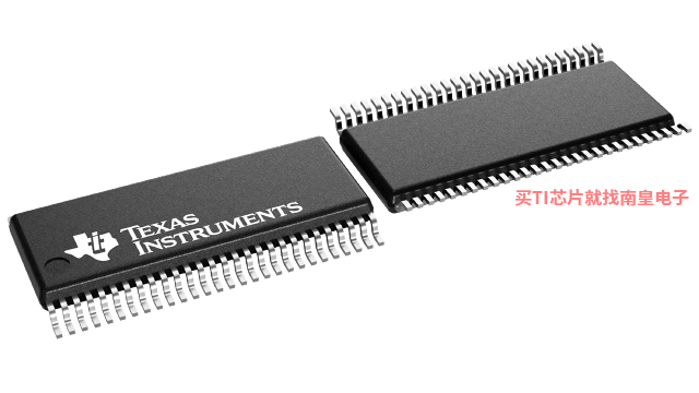
- 制造厂商:TI
- 产品类别:逻辑和电压转换
- 技术类目:缓冲器、驱动器和收发器 - 通用收发器
- 功能描述:具有三态输出的 18 位通用总线驱动器
- 点击这里打开及下载SN74AVC16835的技术文档资料
- TI代理渠道,提供当日发货、严格的质量标准,满足您的目标价格

A Dynamic Output Control (DOC™) circuit is implemented, which, during the transition, initially lowers the output impedance to effectively drive the load and, subsequently, raises the impedance to reduce noise. Figure 1 shows typical VOL vs IOL and VOH vs IOH curves to illustrate the output impedance and drive capability of the circuit. At the beginning of the signal transition, the DOC circuit provides a maximum dynamic drive that is equivalent to a high-drive standard-output device. For more information, refer to the TI application reports, AVC Logic Family Technology and Applications, literature number SCEA006, and Dynamic Output Control (DOC™) Circuitry Technology and Applications, literature number SCEA009.
This 18-bit universal bus driver is operational at 1.2-V to 3.6-V VCC, but is designed specifically for 1.65-V to 3.6-V VCC operation.
Data flow from A to Y is controlled by the output-enable (OE)\ input. The device operates in the transparent mode when the latch-enable (LE) input is high. The A data is latched if the clock (CLK) input is held at a high or low logic level. If LE is low, the A data is stored in the latch/flip-flop on the low-to-high transition of CLK. When OE\ is high, the outputs are in the high-impedance state.
To ensure the high-impedance state during power up or power down, OE\ should be tied to VCC through a pullup resistor; the minimum value of the resistor is determined by the current-sinking capability of the driver.
This device is fully specified for partial-power-down applications using Ioff. The Ioff circuitry disables the outputs, preventing damaging current backflow through the device when it is powered down.
- Member of the Texas Instruments Widebus? Family
- DOC? (Dynamic Output Control) Circuit Dynamically Changes Output Impedance, Resulting in Noise Reduction Without Speed Degradation
- Dynamic Drive Capability Is Equivalent to Standard Outputs With IOH and IOL of ±24 mA at 2.5-V VCC
- Overvoltage-Tolerant Inputs/Outputs Allow Mixed-Voltage-Mode Data Communications
- Ioff Supports Partial-Power-Down Mode Operation
- ESD Protection Exceeds JESD 22
- 2000-V Human-Body Model (A114-A)
- 200-V Machine Model (A115-A)
- Latch-Up Performance Exceeds 100 mA Per JESD 78, Class II
DOC and Widebus are trademarks of Texas Instruments.
- IOL (Max) (mA)
- 24
- IOH (Max) (mA)
- -24
- Technology Family
- AVC
- Rating
- Catalog
- Operating temperature range (C)
- -40 to 85
SN74AVC16835的完整型号有:SN74AVC16835DGVR,以下是这些产品的关键参数及官网采购报价:
SN74AVC16835DGVR,工作温度:-40 to 85,封装:TVSOP (DGV)-56,包装数量MPQ:2000个,MSL 等级/回流焊峰值温度:Level-1-260C-UNLIM,引脚镀层/焊球材料:NIPDAU,TI官网SN74AVC16835DGVR的批量USD价格:1.253(1000+)

SN74AVC16835DGVR,工作温度:-40 to 85,封装:TVSOP (DGV)-56,包装数量MPQ:2000个,MSL 等级/回流焊峰值温度:Level-1-260C-UNLIM,引脚镀层/焊球材料:NIPDAU,TI官网SN74AVC16835DGVR的批量USD价格:1.253(1000+)


