- 制造厂商:TI
- 产品类别:逻辑和电压转换
- 技术类目:电压转换器和电平转换器 - 方向控制型电压转换器
- 功能描述:具有可配置电压转换和三态输出的双位 2-DIR 引脚双电源总线收发器
- 点击这里打开及下载SN74AVC2T245的技术文档资料
- TI代理渠道,提供当日发货、严格的质量标准,满足您的目标价格

This dual-bit noninverting bus transceiver uses two separate configurable power-supply rails. The A port is designed to track VCCA. VCCA accepts any supply voltage from 1.2 V to 3.6 V. The B port is designed to track VCCB. VCCB accepts any supply voltage from 1.2 V to 3.6 V. This allows for universal low-voltage bidirectional translation between any of the 1.2 V, 1.5 V, 1.8 V, 2.5 V, and 3.3 V voltage nodes.
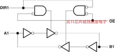
The SN74AVC2T245 is designed for asynchronous communication between two data buses. The logic levels of the direction-control (DIR) input and the output-enable (OE) activate either the B-port outputs or the A-port outputs or place both output ports into the high-impedance mode . The device transmits data from the A bus to the B bus when the B-port outputs are activated and from the B bus to the A bus when the A-port outputs are activated. The input circuitry on both A and B ports always is active and must have a logic HIGH or LOW level applied to prevent excess ICC and ICCZ.
The SN74AVC2T245 control pins (DIR1, DIR2, and OE) are supplied by VCCA.
This device is fully specified for partial-power-down applications using Ioff. The Ioff circuitry disables the outputs, preventing damaging current backflow through the device when it is powered down.
The VCC isolation feature ensures that if either VCC input is at GND, both ports are in the high-impedance state.
To ensure the high-impedance state during power up or power down, OE must be connected to VCC through a pull-up resistor; the minimum value of the resistor is determined by the current-sinking capability of the driver.
- Each Channel Has Independent Direction Control
- Control Inputs VIH/VIL Levels Are Referenced to VCCA Voltage
- Fully Configurable Dual-Rail Design Allows Each Port to Operate Over the Full 1.2 V to 3.6 V Power-Supply Range
- I/Os Are 4.6 V Tolerant
- Ioff Supports Partial-Power-Down Mode Operation
- VCC Isolation Feature - If Either VCC Input is at GND, Both Ports are in High-Impedance State
- Typical Data Rates
- 500 Mbps (1.8 V to 3.3 V Level-Shifting)
- 320 Mbps (<1.8 V to 3.3 V Level-Shifting)
- 320 Mbps (Translate to 2.5 V or 1.8 V)
- 280 Mbps (Translate to 1.5 V)
- 240 Mbps (Translate to 1.2 V)
- Latch-Up Performance Exceeds 100 mA Per JESD 78, Class II
- ESD Protection Exceeds JESD 22
- 5000 V Human-Body Model (A114-A)
- 200 V Machine Model (A115-A)
- 1500 V Charged-Device Model (C101)
- Technology Family
- AVC
- Applications
- JTAG
- Bits (#)
- 2
- High input voltage (Min) (Vih)
- 0.78
- High input voltage (Max) (Vih)
- 3.6
- Vout (Min) (V)
- 1.2
- Vout (Max) (V)
- 3.6
- IOH (Max) (mA)
- -12
- IOL (Max) (mA)
- 12
- Rating
- Catalog
SN74AVC2T245的完整型号有:SN74AVC2T245RSWR,以下是这些产品的关键参数及官网采购报价:
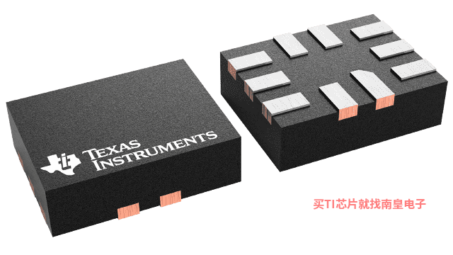
SN74AVC2T245RSWR,工作温度:-40 to 85,封装:UQFN (RSW)-10,包装数量MPQ:3000个,MSL 等级/回流焊峰值温度:Level-1-260C-UNLIM,引脚镀层/焊球材料:NIPDAU,TI官网SN74AVC2T245RSWR的批量USD价格:.323(1000+)

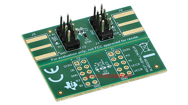
AXC2T-SMALLPKGEVM ― AXC2T-SMALLPKGEVM
This EVM is designed to support DTM and RSW packages for the AXC and LVC family of DIR controlled bidirectional devices. The AXC and AVC devices belong to the low voltage direction controlled translation family with operating voltage from 0.65V to 3.6V (AXC) and 1.2 to 3.6 (AVC) with 12mA of drive (...)EVMK2GX ― 66AK2Gx 1GHz 评估模块
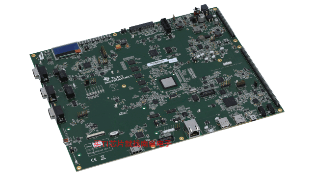
EVMK2GX(也称为“K2G”)1GHz 评估模块 (EVM) 可以让开发人员迅速开始评估 66AK2Gx 处理器系列,并加速音频、工业电机控制、智能电网保护和其他高可靠性实时计算密集型应用的开发。 66AK2Gx 与基于 KeyStone 的现有 SoC 器件类似,可以让 DSP 和 ARM 内核控制系统中的所有内存和外设。此架构有助于最大限度地提高软件灵活性,并可以在其中实现以 DSP 或 ARM 为中心的系统设计。
无论是 Linux 还是 TI-RTOS 操作系统,处理器 SDK 均支持此 EVM,而且此 EVM 采用 USB、PCIe 和千兆位以太网等主要外设。 (...)
SN74AVC2T245 IBIS Model
此参考设计基于 HEIDENHAIN EnDat 2.2 标准针对位置或旋转编码器实现了 EnDat 2.2 主协议栈和硬件接口。此设计由 EnDat 2.2 主协议栈、使用 RS-485 收发器的半双工通信,以及在 Sitara AM437x 工业开发工具包上实现的线路终端组成。此设计经过充分测试,符合 HEIDENHAIN EnDat 2.2 标准。除了 EnDat 位置反馈之外,AM437x IDK 还能够支持工业通信和电机驱动,如 AM437x 单芯片电机控制设计指南中所述。TIDA-00403 ― 采用 TLV320AIC3268 miniDSP 编解码器的超声波测距参考设计
TIDA-00403 参考设计使用针对超声测距解决方案的现成的 EVM,该解决方案使用 TLV320AIC3268 miniDSP 内的算法。通过将该设计与 TI 的 PurePath Studio 设计套件结合使用,只需点击鼠标即可设计出一个用户可配置的稳健的超声测距系统。用户可以修改超声波脉冲生成特性以及检测算法以适合工业和测量应用中的特定使用情况,从而让用户能解决其他固定功能传感器的限制,同时增加测量的可靠性。TLV320AIC3268 上的两个 GPIO 被自动触发,表明已发出并接收到超声波脉冲。通过利用主机 MCU 监测这些 GPIO 可以提取出飞行时间。


