- ���쳧�̣�TI
- ��Ʒ������͵�ѹת��
- ������Ŀ����ѹת�����͵�ƽת���� - ��������͵�ѹת����
- �������������п����õ�ѹת������̬����������� 8 λ˫��Դ�����շ���
- ������������SN74AVC8T245-Q1�ļ����ĵ�����
- TI�����������ṩ���շ������ϸ������������������Ŀ��۸�

The SN74AVC8T245-Q1 is an 8-bit noninverting bus transceiver that uses two separate configurable power-supply rails. The SN74AVC8T245-Q1 operation is optimimal with VCCA and VCCB set at
1.4 V to 3.6 V. It is operational with VCCA and VCCB as low as 1.2 V. The A port is designed to track VCCA. VCCA accepts any supply voltage from 1.2 V to 3.6 V. The B port is designed to track VCCB. VCCB accepts any supply voltage from 1.2 V to 3.6 V. This allows for universal low-voltage bidirectional translation between any of the 1.2-V, 1.5-V, 1.8-V, 2.5-V, and 3.3-V voltage nodes.
The SN74AVC8T245 design enables asynchronous communication between data buses. The device transmits data from the A bus to the B bus or from the B bus to the A bus, depending on the logic level at the direction-control (DIR) input. One can use the output-enable (OE) input to disable the outputs so the buses are effectively isolated.
In the SN74AVC8T245 design, VCCA supplies the control pins (DIR and OE).
This device specification covers partial-power-down applications using Ioff. The Ioff circuitry disables the outputs when the device is powered down. This inhibits current backflow into the device which prevents damage to the device.
The VCC isolation feature ensures that if either VCC input is at GND, both ports are in the high-impedance state.
To ensure the high-impedance state during power up or power down, tie OE to VCC through a pullup resistor; the current-sinking capability of the driver determines the minimum value of the resistor.
- Qualified for Automotive Applications
- AEC Q100 Test Guidance With the Following Results:
- Device Temperature Grade 1: �C40��C to +125��C Ambient Operating Temperature Range
- Device HBM ESD Classification Level H2
- Device CDM ESD Classification Level C3B
- Control Inputs VIH and VIL Levels Are Referenced to VCCA Voltage
- VCC Isolation Feature �C If Either VCC Input Is at GND, All I/O Ports Are in the High-Impedance State
- Ioff Supports Partial Power-Down-Mode Operation
- Fully Configurable Dual-Rail Design Allows Each Port to Operate Over the Full 1.4-V to 3.6-V Power-Supply Range
- I/Os Are 4.6-V Tolerant
- Maximum Data Rates
- 170 Mbps (VCCA < 1.8 V or VCCB < 1.8 V)
- 320 Mbps (VCCA �� 1.8 V and VCCB �� 1.8 V)
- Latch-Up Performance Exceeds 100 mA per JESD 78, Class II
- Technology Family
- AVC
- Applications
- RGMII
- Bits (#)
- 8
- High input voltage (Min) (Vih)
- 0.78
- High input voltage (Max) (Vih)
- 3.6
- Vout (Min) (V)
- 1.2
- Vout (Max) (V)
- 3.6
- IOH (Max) (mA)
- -12
- IOL (Max) (mA)
- 12
- Rating
- Automotive
SN74AVC8T245-Q1�������ͺ��У�CAVC8T245QRHLRQ1��SN74AVC8T245QPWRQ1����������Щ��Ʒ�Ĺؼ������������ɹ����ۣ�
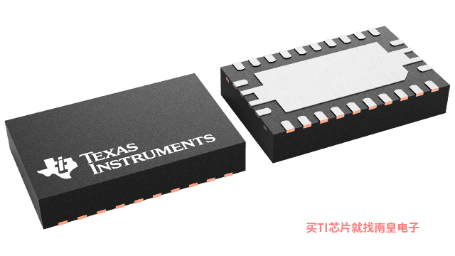
CAVC8T245QRHLRQ1�������¶ȣ�-40 to 125����װ��VQFN (RHL)-24����װ����MPQ��1000����MSL �ȼ�/��������ֵ�¶ȣ�Level-2-260C-1 YEAR�����ŶƲ�/������ϣ�NIPDAU��TI����CAVC8T245QRHLRQ1������USD�۸�.611��1000+��
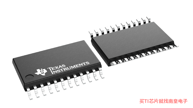
SN74AVC8T245QPWRQ1�������¶ȣ�-40 to 125����װ��TSSOP (PW)-24����װ����MPQ��2000����MSL �ȼ�/��������ֵ�¶ȣ�Level-3-260C-168 HR�����ŶƲ�/������ϣ�NIPDAU��TI����SN74AVC8T245QPWRQ1������USD�۸�.586��1000+��

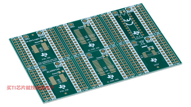
14-24-LOGIC-EVM �� ֧�� 14 �� 24 ���� PW��DB��D��DW��NS��DYY �� DGV ��װ��ͨ���� EVM
�� EVM �������֧�ֲ��� 14 �� 24 ���� D��DW��DB��NS��PW��DYY �� DGV ��װ���κ���������
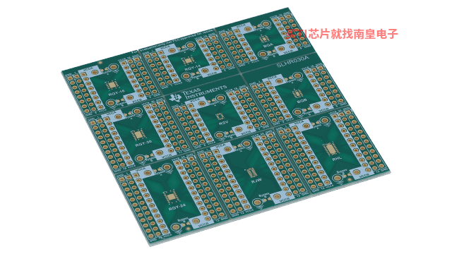
14-24-NL-LOGIC-EVM �� Generic 14 through 24 pin non-leaded package evaluation module
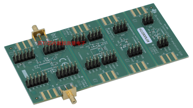
Flexible EVM designed to support any logic or translation device that has a BQA, BQB, RGY (14-24 pin), RSV, RJW, or RHL package.AVCLVCDIRCNTRL-EVM �� �����ڷ������˫��ת��������֧�� AVC �� LVC ��ͨ�� EVM
��ͨ�� EVM ּ��֧�� 1��2��4 �� 8 ͨ�� LVC �� AVC �������ת����������������ͬ������ͨ��֧�����߱��ֺ����� Q1 ������AVC �ǵ͵�ѹת������������ 12mA �Ľϵ�����ǿ�ȡ�LVC �� 1.65 �� 5.5V �Ľϸߵ�ѹת������������ 32mA �Ľϸ�����ǿ�ȡ�