- 制造厂商:TI
- 产品类别:逻辑和电压转换
- 技术类目:电压转换器和电平转换器 - 方向控制型电压转换器
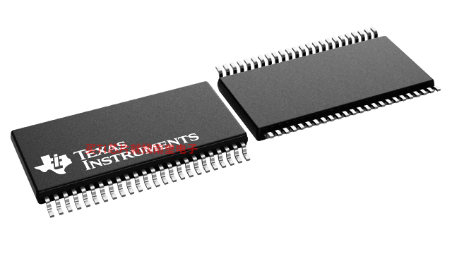
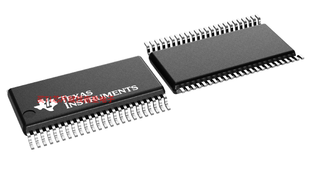
- 功能描述:具有可配置转换和三态输出的 16 位双电源总线收发器
- 点击这里打开及下载SN74AVCB164245的技术文档资料
- TI代理渠道,提供当日发货、严格的质量标准,满足您的目标价格

This 16-bit (dual-octal) noninverting bus transceiver uses two separate configurable power-supply rails. The A port is designed to track VCCA. VCCA accepts any supply voltage from 1.4 V to 3.6 V. The B port is designed to track VCCB. VCCB accepts any supply voltage from 1.4 V to 3.6 V. This allows for universal low-voltage bidirectional translation between any of the 1.5-V, 1.8-V, 2.5-V, and 3.3-V voltage nodes.
The SN74AVCB164245 is designed for asynchronous communication between data buses. The device transmits data from the A bus to the B bus or from the B bus to the A bus, depending on the logic level at the direction-control (DIR) input. The output-enable (OE) input can be used to disable the outputs so the buses are effectively isolated.
The SN74AVCB164245 is designed so that the control pins (1DIR, 2DIR, 1OE, and 2OE) are supplied by VCCB.
To ensure the high-impedance state during power up or power down, OE should be tied to VCCB through a pullup resistor; the minimum value of the resistor is determined by the current-sinking capability of the driver.
This device is fully specified for partial-power-down applications using Ioff. The Ioff circuitry disables the outputs, preventing damaging current backflow through the device when it is powered down. If either VCC input is at GND, both ports are in the high-impedance state.
- Member of the Texas Instruments Widebus? Family
- DOC? Circuitry Dynamically Changes Output Impedance, Resulting in Noise Reduction Without Speed Degradation
- Dynamic Drive Capability Is Equivalent to Standard Outputs With IOH and IOL of ±24 mA at 2.5-V VCC
- Control Inputs VIH/VIL Levels Are Referenced to VCCB Voltage
- If Either VCC Input Is at GND, Both Ports Are in the High-Impedance State
- Overvoltage-Tolerant Inputs/Outputs Allow Mixed-Voltage-Mode Data Communications
- Ioff Supports Partial-Power-Down Mode Operation
- Fully Configurable Dual-Rail Design Allows Each Port to Operate Over Full 1.4-V to 3.6-V Power-Supply Range
- Latch-Up Performance Exceeds 100 mA Per JESD 78, Class II
- ESD Protection Exceeds JESD 22
- 2000-V Human-Body Model (A114-A)
- 200-V Machine Model (A115-A)
- 1000-V Charged-Device Model (C101)
Widebus, DOC are trademarks of Texas Instruments.
- Technology Family
- AVC
- Bits (#)
- 16
- High input voltage (Min) (Vih)
- 0.91
- High input voltage (Max) (Vih)
- 3.6
- Vout (Min) (V)
- 1.4
- Vout (Max) (V)
- 3.6
- IOH (Max) (mA)
- -12
- IOL (Max) (mA)
- 12
- Rating
- Catalog
SN74AVCB164245的完整型号有:SN74AVCB164245GR、SN74AVCB164245VR,以下是这些产品的关键参数及官网采购报价:
SN74AVCB164245GR,工作温度:-40 to 85,封装:TSSOP (DGG)-48,包装数量MPQ:2000个,MSL 等级/回流焊峰值温度:Level-1-260C-UNLIM,引脚镀层/焊球材料:NIPDAU,TI官网SN74AVCB164245GR的批量USD价格:1.294(1000+)
SN74AVCB164245VR,工作温度:-40 to 85,封装:TVSOP (DGV)-48,包装数量MPQ:2000个,MSL 等级/回流焊峰值温度:Level-1-260C-UNLIM,引脚镀层/焊球材料:NIPDAU,TI官网SN74AVCB164245VR的批量USD价格:1.109(1000+)

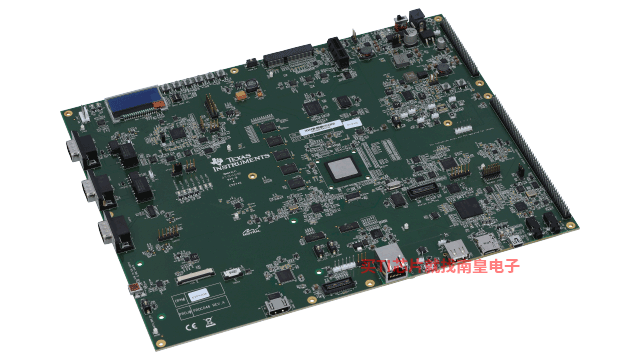
EVMK2GX ― 66AK2Gx 1GHz 评估模块
EVMK2GX(也称为“K2G”)1GHz 评估模块 (EVM) 可以让开发人员迅速开始评估 66AK2Gx 处理器系列,并加速音频、工业电机控制、智能电网保护和其他高可靠性实时计算密集型应用的开发。 66AK2Gx 与基于 KeyStone 的现有 SoC 器件类似,可以让 DSP 和 ARM 内核控制系统中的所有内存和外设。此架构有助于最大限度地提高软件灵活性,并可以在其中实现以 DSP 或 ARM 为中心的系统设计。
无论是 Linux 还是 TI-RTOS 操作系统,处理器 SDK 均支持此 EVM,而且此 EVM 采用 USB、PCIe 和千兆位以太网等主要外设。 (...)


