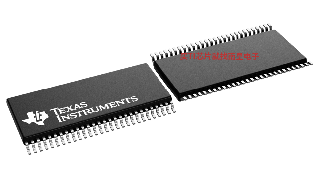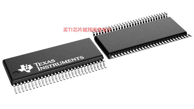
- 制造厂商:TI
- 产品类别:逻辑和电压转换
- 技术类目:电压转换器和电平转换器 - 方向控制型电压转换器
- 功能描述:具有可配置电压转换和三态输出的 20 位双电源总线收发器
- 点击这里打开及下载SN74AVCH20T245的技术文档资料
- TI代理渠道,提供当日发货、严格的质量标准,满足您的目标价格

This 20-bit noninverting bus transceiver uses two separate configurable power-supply rails. The SN74AVCH20T245 is optimized to operate with VCCA/VCCB set at 1.4 V to 3.6 V. It is operational with VCCA/VCCB as low as 1.2 V. The A port is designed to track VCCA. VCCA accepts any supply voltage from 1.2 V to 3.6 V. The B port is designed to track VCCB. VCCB accepts any supply voltage from 1.2 V to 3.6 V. This allows for universal low-voltage bidirectional translation between any of the 1.2-V, 1.5-V, 1.8-V, 2.5-V, and 3.3-V voltage nodes.
The SN74AVCH20T245 is designed for asynchronous communication between data buses. The device transmits data from the A bus to the B bus or from the B bus to the A bus, depending on the logic level at the direction-control (DIR) input. The output-enable (OE)\ input can be used to disable the outputs so that the buses are effectively isolated.
The SN74AVCH20T245 is designed so that the control (1DIR, 2DIR, 1OE\, and 2OE\) inputs are supplied by VCCA.
This device is fully specified for partial-power-down applications using Ioff. The Ioff circuitry disables the outputs, preventing damaging current backflow through the device when it is powered down.
The VCC isolation feature ensures that if either VCC input is at GND, both outputs are in the high-impedance state. The bus-hold circuitry on the powered-up side always stays active.
Active bus-hold circuitry holds unused or undriven inputs at a valid logic state. Use of pullup or pulldown resistors with the bus-hold circuitry is not recommended.
To ensure the high-impedance state during power up or power down, OE\ should be tied to VCC through a pullup resistor; the minimum value of the resistor is determined by the current-sinking capability of the driver.
- Control Inputs VIH/VIL Levels are Referenced to VCCA Voltage
- VCC Isolation Feature - If Either VCC Input Is at GND, Both Ports Are in the High-Impedance State
- Overvoltage-Tolerant Inputs/Outputs Allow Mixed-Voltage-Mode Data Communications
- Fully Configurable Dual-Rail Design Allows Each Port to Operate Over the Full 1.2-V to 3.6-V Power-Supply Range
- Ioff Supports Partial-Power-Down Mode Operation
- I/Os Are 4.6-V Tolerant
- Bus Hold on Data Inputs Eliminates the Need for External Pullup/Pulldown Resistors
- Max Data Rates
- 380 Mbps (1.8-V to 3.3-V Translation)
- 260 Mbps (1.8-V to 3.3-V Translation)
- 260 Mbps (Translate to 2.5 V)
- 210 Mbps (Translate to 1.8 V)
- 120 Mbps (Translate to 1.5 V)
- 100 Mbps (Translate to 1.2 V)
- Latch-Up Performance Exceeds 100 mA Per JESD 78, Class II
- ESD Protection Exceeds JESD 22
- 8000-V Human-Body Model (A114-A)
- 200-V Machine Model (A115-A)
- 1000-V Charged-Device Model (C101)
- Technology Family
- AVC
- Bits (#)
- 20
- High input voltage (Min) (Vih)
- 0.8
- High input voltage (Max) (Vih)
- 3.6
- Vout (Min) (V)
- 1.2
- Vout (Max) (V)
- 3.6
- IOH (Max) (mA)
- -12
- IOL (Max) (mA)
- 12
- Rating
- Catalog
SN74AVCH20T245的完整型号有:SN74AVCH20T245GR、SN74AVCH20T245VR,以下是这些产品的关键参数及官网采购报价:
SN74AVCH20T245GR,工作温度:-40 to 85,封装:TSSOP (DGG)-56,包装数量MPQ:2000个,MSL 等级/回流焊峰值温度:Level-1-260C-UNLIM,引脚镀层/焊球材料:NIPDAU,TI官网SN74AVCH20T245GR的批量USD价格:.933(1000+)
SN74AVCH20T245VR,工作温度:-40 to 85,封装:TVSOP (DGV)-56,包装数量MPQ:2000个,MSL 等级/回流焊峰值温度:Level-1-260C-UNLIM,引脚镀层/焊球材料:NIPDAU,TI官网SN74AVCH20T245VR的批量USD价格:.933(1000+)


