- ���쳧�̣�TI
- ��Ʒ������͵�ѹת��
- ������Ŀ����ѹת�����͵�ƽת���� - ��������͵�ѹת����
- �������������ж��� DIR ���ƺ���̬����������� 2 λ˫��Դ��ѹ��ƽת��
- ������������SN74AXC2T245-Q1�ļ����ĵ�����
- TI�����������ṩ���շ������ϸ������������������Ŀ��۸�

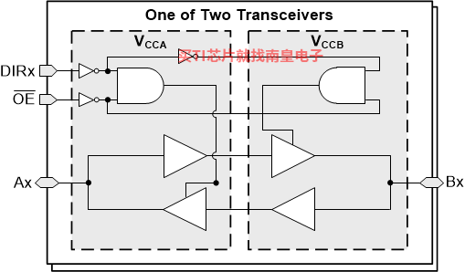
The SN74AXC2T245-Q1 is a two-bit noninverting bus transceiver that uses two individually configurable power-supply rails. The device is operational with both VCCA and VCCB supplies as low as 0.65 V. The A port is designed to track VCCA, which accepts any supply voltage from 0.65 V to 3.6 V. The B port is designed to track VCCB, which also accepts any supply voltage from 0.65 V to 3.6 V. Additionally the SN74AXC2T245-Q1 is compatible with a single-supply system.
The SN74AXC2T245-Q1 device is designed for asynchronous communication between data buses. The device transmits data from the A bus to the B bus or from the B bus to the A bus, depending on the logic level of the direction-control inputs (DIRx). The SN74AXC2T245-Q1 device is designed so the control pin (DIR) is referenced to VCCA.
This device is fully specified for partial-power-down applications using the Ioff current. The Ioff protection circuitry ensures that no excessive current is drawn from or to an input, output, or combined I/O that is biased to a specific voltage while the device is powered down.
The VCC isolation feature ensures that if either VCCA or VCCB is less than 100 mV, both I/O ports enter a high-impedance state by disabling their outputs.
Glitch-free power supply sequencing allows either supply rail to be powered on or off in any order while providing robust power sequencing performance.
- AEC-Q100 automotive qualified
- Fully configurable dual-rail design allows each port to operate with a power supply range rrom 0.65 V to 3.6 V
- Operating temperature from �C40��C to +125��C
- DIR control input for each channel
- Glitch-free power supply sequencing
- Up to 380 Mbps support when translating from 1.8 V to 3.3 V
- VCC isolation feature
- If either VCC input is below 100 mV, all I/O outputs are disabled and become high-impedance
- Ioff supports partial-power-down mode operation
- Compatible with AVC-family level shifters
- Latch-up performance exceeds 100 mA per JESD 78, class II
- ESD protection exceeds JEDEC JS-001
- 8000-V Human-body model
- 1000-V Charged-device model
- Technology Family
- AXC
- Applications
- UART, JTAG
- Bits (#)
- 2
- High input voltage (Min) (Vih)
- 0.45
- High input voltage (Max) (Vih)
- 3.6
- Vout (Min) (V)
- 0.65
- Vout (Max) (V)
- 3.6
- IOH (Max) (mA)
- -12
- IOL (Max) (mA)
- 12
- Rating
- Automotive
SN74AXC2T245-Q1�������ͺ��У�CAXC2T245QRSWRQ1����������Щ��Ʒ�Ĺؼ������������ɹ����ۣ�
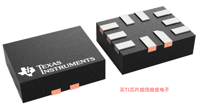
CAXC2T245QRSWRQ1�������¶ȣ�-40 to 125����װ��UQFN (RSW)-10����װ����MPQ��3000����MSL �ȼ�/��������ֵ�¶ȣ�Level-1-260C-UNLIM�����ŶƲ�/������ϣ�NIPDAU��TI����CAXC2T245QRSWRQ1������USD�۸�.357��1000+��

AXC2T-SMALLPKGEVM �� AXC2T-SMALLPKGEVM
This EVM is designed to support DTM and RSW packages for the AXC and LVC family of DIR controlled bidirectional devices. The AXC and AVC devices belong to the low voltage direction controlled translation family with operating voltage from 0.65V to 3.6V (AXC) and 1.2 to 3.6 (AVC) with 12mA of drive (...)


