- 制造厂商:TI
- 产品类别:开关与多路复用器
- 技术类目:模拟开关和多路复用器
- 功能描述:具有预充电输出的 3.3V、1:1 (SPST)、10 通道通用 FET 总线开关
- 点击这里打开及下载SN74CB3Q6800的技术文档资料
- TI代理渠道,提供当日发货、严格的质量标准,满足您的目标价格

The SN74CB3Q6800 is a high-bandwidth FET bus switch utilizing a charge pump to elevate the gate voltage of the pass transistor, providing a low and flat ON-state resistance (ron). The low and flat ON-state resistance allows for minimal propagation delay and supports rail-to-rail switching on the data input/output (I/O) ports. The device also features low data I/O capacitance to minimize capacitive loading and signal distortion on the data bus. Specifically designed to support high-bandwidth applications, the SN74CB3Q6800 provides an optimized interface solution ideally suited for broadband communications, networking, and data-intensive computing systems.
The SN74CB3Q6800 is a 10-bit bus switch with a single output-enable (ON\) input. When ON\ is low, the 10-bit bus switch is ON and the A port is connected to the B port, allowing bidirectional data flow between ports. When ON\ is high, the 10-bit bus switch is OFF and a high-impedance state exists between the A and B ports. The B port is precharged to bias voltage (BIASV) through the equivalent of a 10-k resistor when ON\ is high, or if the device is powered down (VCC = 0 V).
During insertion (or removal) of a card into (or from) an active bus, the card’s output voltage may be close to GND. When the connector pins make contact, the card’s parasitic capacitance tries to force the bus signal to GND, creating a possible glitch on the active bus. This glitching effect can be reduced by using a bus switch with precharged bias voltage (BIASV) of the bus switch equal to the input threshold voltage level of the receivers on the active bus. This method will ensure that any glitch produced by insertion (or removal) of the card will not cross the input threshold region of the receivers on the active bus, minimizing the effects of live-insertion noise.
This device is fully specified for partial-power-down applications using Ioff. The Ioff circuitry prevents damaging current backflow through the device when it is powered down. The device has isolation during power off.
To ensure the high-impedance state during power up or power down, ON\ should be tied to VCC through a pullup resistor; the minimum value of the resistor is determined by the current-sinking capability of the driver.
- High-Bandwidth Data Path (Up To 500 MHz)
- 5-V Tolerant I/Os with Device Powered-Up or Powered-Down
- Low and Flat ON-State Resistance (ron) Characteristics Over Operating Range (ron = 4.5 Typical)
- Rail-to-Rail Switching on Data I/O Ports
- 0- to 5-V Switching With 3.3-V VCC
- 0- to 3.3-V Switching With 2.5-V VCC
- B-Port Outputs Are Precharged by Bias Voltage (BIASV) to Minimize Signal Distortion During Live Insertion and Hot-Plugging
- Supports PCI Hot Plug
- Bidirectional Data Flow, With Near-Zero Propagation Delay
- Low Input/Output Capacitance Minimizes Loading and Signal Distortion (Cio(OFF) = 3.5 pF Typical)
- Fast Switching Frequency (fON\= 20 MHz Max)
- Data and Control Inputs Provide Undershoot Clamp Diodes
- Low Power Consumption (ICC = 0.75 mA Typical)
- VCC Operating Range From 2.3 V to 3.6 V
- Data I/Os Support 0 to 5-V Signaling Levels (0.8-V, 1.2-V, 1.5-V, 1.8-V, 2.5-V, 3.3-V, 5-V)
- Control Inputs Can be Driven by TTL or 5-V/3.3-V CMOS Outputs
- Ioff Supports Partial-Power-Down Mode Operation
- Latch-Up Performance Exceeds 100 mA Per JESD 78, Class II
- ESD Performance Tested Per JESD 22
- 2000-V Human-Body Model (A114-B, Class II)
- 1000-V Charged-Device Model (C101)
- Supports Both Digital and Analog Applications: PCI Interface, Differential Signal Interface, Memory Interleaving, Bus Isolation, Low-Distortion Signal Gating
For additional information regarding the performance characteristics of the CB3Q family, refer to the TI application report, CBT-C, CB3T, and CB3Q Signal-Switch Families, literature number SCDA008.
- Configuration
- 1:1 SPST
- Number of channels (#)
- 10
- Power supply voltage - single (V)
- 2.5, 3.3
- Protocols
- Analog
- Ron (Typ) (Ohms)
- 4.5
- CON (Typ) (pF)
- 9
- Bandwidth (MHz)
- 500
- Operating temperature range (C)
- -40 to 85
- Features
- Powered-off protection, Supports input voltage beyond supply
- Input/output continuous current (Max) (mA)
- 64
- Rating
- Catalog
- Supply current (Typ) (uA)
- 750
SN74CB3Q6800的完整型号有:SN74CB3Q6800DBQR、SN74CB3Q6800DGVR、SN74CB3Q6800PW、SN74CB3Q6800PWR,以下是这些产品的关键参数及官网采购报价:
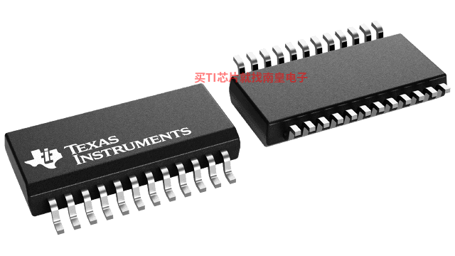
SN74CB3Q6800DBQR,工作温度:-40 to 85,封装:SSOP (DBQ)-24,包装数量MPQ:2500个,MSL 等级/回流焊峰值温度:Level-2-260C-1 YEAR,引脚镀层/焊球材料:NIPDAU,TI官网SN74CB3Q6800DBQR的批量USD价格:.251(1000+)
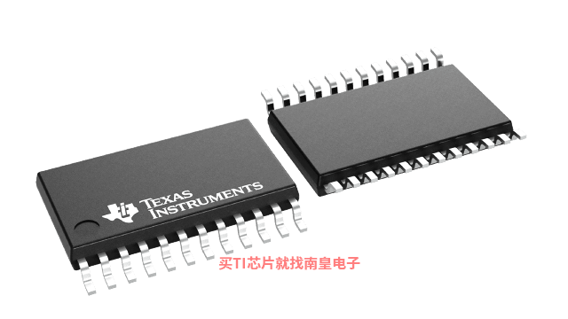
SN74CB3Q6800DGVR,工作温度:-40 to 85,封装:TVSOP (DGV)-24,包装数量MPQ:2000个,MSL 等级/回流焊峰值温度:Level-1-260C-UNLIM,引脚镀层/焊球材料:NIPDAU,TI官网SN74CB3Q6800DGVR的批量USD价格:.228(1000+)
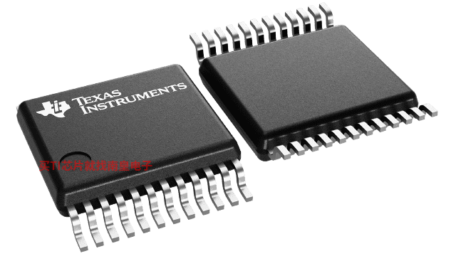
SN74CB3Q6800PW,工作温度:-40 to 85,封装:TSSOP (PW)-24,包装数量MPQ:60个,MSL 等级/回流焊峰值温度:Level-1-260C-UNLIM,引脚镀层/焊球材料:NIPDAU,TI官网SN74CB3Q6800PW的批量USD价格:.274(1000+)
SN74CB3Q6800PWR,工作温度:-40 to 85,封装:TSSOP (PW)-24,包装数量MPQ:2000个,MSL 等级/回流焊峰值温度:Level-1-260C-UNLIM,引脚镀层/焊球材料:NIPDAU,TI官网SN74CB3Q6800PWR的批量USD价格:.228(1000+)

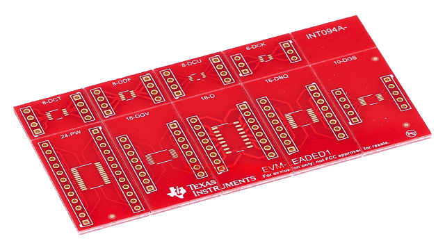
LEADED-ADAPTER1 ― 用于快速测试 TI 5、8、10、16 和 24 引脚引线式封装的表面贴装转 DIP 接头适配器
EVM-LEADED1 板可对 TI 的常见引线式封装进行快速测试和电路板试验。该评估板具有足够的空间,可将 TI 的 D、DBQ、DCT、DCU、DDF、DGS、DGV 和 PW 表面贴装封装转换为 100mil DIP 接头。