- 制造厂商:TI
- 产品类别:开关与多路复用器
- 技术类目:模拟开关和多路复用器
- 功能描述:具有电平转换器的 3.3V、1:1 (SPST)、单通道 FET 总线开关
- 点击这里打开及下载SN74CB3T1G125的技术文档资料
- TI代理渠道,提供当日发货、严格的质量标准,满足您的目标价格

The SN74CB3T1G125 is a high-speed TTL-compatible FET bus switch with low ON-state resistance (ron), allowing for minimal propagation delay. The device fully supports mixed-mode signal operation on all data I/O ports by providing voltage translation that tracks VCC. The SN74CB3T1G125 supports systems using 5-V TTL, 3.3-V LVTTL, and 2.5-V CMOS switching standards, as well as user-defined switching levels.
The SN74CB3T1G125 is a 1-bit bus switch with a single ouput-enable (OE) input. When OE is low, the bus switch is ON, and the A port is connected to the B port, allowing bidirectional data flow between ports. When OE is high, the bus switch is OFF, and a high-impedance state exists between the A and B ports.
This device is fully specified for partial-power-down applications using Ioff. The Ioff feature ensures that damaging current will not backflow through the device when it is powered down. The device has isolation during power off.
To ensure the high-impedance state during power up or power down, OE should be tied to VCC through a pullup resistor; the minimum value of the resistor is determined by the current-sinking capability of the driver.
- Output Voltage Translation Tracks VCC
- Supports Mixed-Mode Signal Operation on All Data I/O Ports
- 5-V Input Down to 3.3-V Output Level Shift With 3.3-V VCC
- 5-V/3.3-V Input Down to 2.5-V Output Level Shift With 2.5-V VCC
- 5-V-Tolerant I/Os, With Device Powered Up or Powered Down
- Bidirectional Data Flow With Near-Zero Propagation Delay
- Low ON-State Resistance (ron) Characteristics (ron = 5 Typ)
- Low Input/Output Capacitance Minimizes Loading (Cio(OFF) = 5 pF Typ)
- Data and Control Inputs Provide Undershoot Clamp Diodes
- Low Power Consumption (ICC = 20 μA Max)
- VCC Operating Range From 2.3 V to 3.6 V
- Data I/Os Support 0- to 5-V Signaling Levels (0.8 V, 1.2 V, 1.5 V, 1.8 V, 2.5 V, 3.3 V, 5 V)
- Control Inputs Can Be Driven by TTL or 5-V/3.3-V CMOS Outputs
- Ioff Supports Partial-Power-Down Mode Operation
- Latch-Up Performance Exceeds 250 mA Per JESD 17
- ESD Performance Tested Per JESD 22
- 2000-V Human-Body Model (A114-B, Class II)
- 1000-V Charged-Device Model (C101)
- Supports Digital Applications: Level Translation, USB Interface, Bus Isolation
- Ideal for Low-Power Portable Equipment
- Configuration
- 1:1 SPST
- Number of channels (#)
- 1
- Power supply voltage - single (V)
- 2.5, 3.3
- Protocols
- Analog
- Ron (Typ) (Ohms)
- 5
- CON (Typ) (pF)
- 12
- ON-state leakage current (Max) (μA)
- 20
- Operating temperature range (C)
- -40 to 85
- Features
- Powered-off protection, Signal path translation
- Input/output continuous current (Max) (mA)
- 128
- Rating
- Catalog
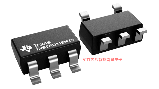
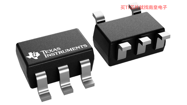
SN74CB3T1G125的完整型号有:74CB3T1G125DBVRG4、SN74CB3T1G125DBVR、SN74CB3T1G125DCKR,以下是这些产品的关键参数及官网采购报价:
74CB3T1G125DBVRG4,工作温度:-40 to 85,封装:SOT-23 (DBV)-5,包装数量MPQ:3000个,MSL 等级/回流焊峰值温度:Level-1-260C-UNLIM,引脚镀层/焊球材料:NIPDAU,TI官网74CB3T1G125DBVRG4的批量USD价格:.437(1000+)
SN74CB3T1G125DBVR,工作温度:-40 to 85,封装:SOT-23 (DBV)-5,包装数量MPQ:3000个,MSL 等级/回流焊峰值温度:Level-1-260C-UNLIM,引脚镀层/焊球材料:NIPDAU,TI官网SN74CB3T1G125DBVR的批量USD价格:.258(1000+)
SN74CB3T1G125DCKR,工作温度:-40 to 85,封装:SC70 (DCK)-5,包装数量MPQ:3000个,MSL 等级/回流焊峰值温度:Level-1-260C-UNLIM,引脚镀层/焊球材料:SN,TI官网SN74CB3T1G125DCKR的批量USD价格:.38(1000+)

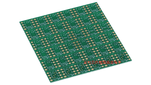
DIP-ADAPTER-EVM ― DIP 适配器评估模块
借助 DIP-Adapter-EVM 加快运算放大器的原型设计和测试,该 EVM 有助于快速轻松地连接小型表面贴装 IC 并且价格低廉。您可以使用随附的 Samtec 端子板连接任何受支持的运算放大器,或者将这些端子板直接连接至现有电路。
DIP-Adapter-EVM 套件支持六种常用的业界通用封装,包括:
- D 和 U (SOIC-8)
- PW (TSSOP-8)
- DGK(MSOP-8、VSSOP-8)
- DBV(SOT23-6、SOT23-5 和 SOT23-3)
- DCK(SC70-6 和 SC70-5)
- DRL (SOT563-6)


