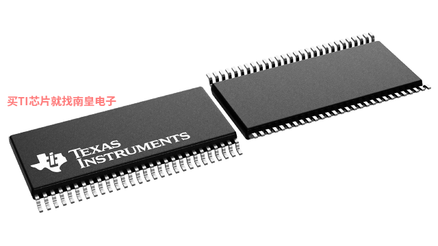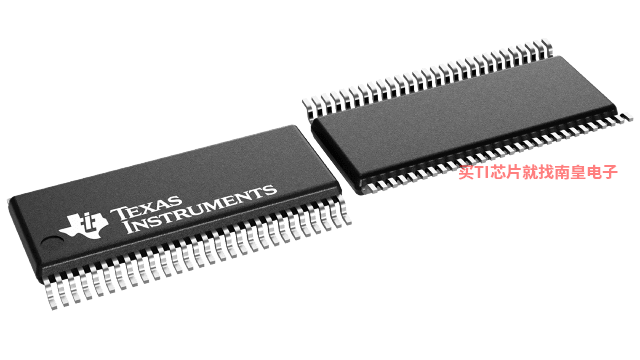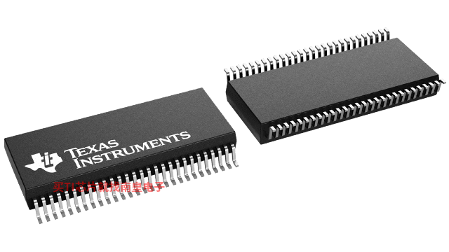
- 制造厂商:TI
- 产品类别:开关与多路复用器
- 技术类目:模拟开关和多路复用器
- 功能描述:具有 –2V 下冲保护的 5V、交叉点/交换、24 通道 FET 总线开关
- 点击这里打开及下载SN74CBT16212C的技术文档资料
- TI代理渠道,提供当日发货、严格的质量标准,满足您的目标价格

The SN74CBT16212C is a high-speed TTL-compatible FET bus-exchange switch with low ON-state resistance (ron), allowing for minimal propagation delay. Active Undershoot-Protection Circuitry on the A and B ports of the SN74CBT16212C provides protection for undershoot up to –2 V by sensing an undershoot event and ensuring that the switch remains in the proper OFF state.
The SN74CBT16212C operates as a 24-bit bus switch, or as a 12-bit bus-exchange that provides data exchanging between four signal ports. The select (S0, S1, S2) inputs control the data path of the bus-exchange switch. When the bus-exchange switch is ON, the A port is connected to the B port, allowing bidirectional data flow between ports. When the bus-exchange switch is disabled, a high-impedance state exists between the A and B ports.
This device is fully specified for partial-power-down applications using Ioff. The Ioff feature ensures that damaging current will not backflow through the device when it is powered down. The device has isolation during power off.
To ensure the high-impedance state during power up or power down, each select input should be tied to GND through a pulldown resistor; the minimum value of the resistor is determined by the current-sourcing capability of the driver.
- Member of the Texas Instruments Widebus? Family
- Undershoot Protection for Off-Isolation on A and B Ports Up To –2 V
- Bidirectional Data Flow, With Near-Zero Propagation Delay
- Low ON-State Resistance (ron) Characteristics (ron = 3 Typical)
- Low Input/Output Capacitance Minimizes Loading and Signal Distortion (Cio(OFF) = 8 pF Typical)
- Data and Control Inputs Provide Undershoot Clamp Diodes
- Low Power Consumption (ICC = 5 μA Max)
- VCC Operating Range From 4 V to 5.5 V
- Data I/Os Support 0 to 5-V Signaling Levels (0.8-V, 1.2-V, 1.5-V, 1.8-V, 2.5-V, 3.3-V, 5-V)
- Control Inputs Can Be Driven by TTL or 5-V/3.3-V CMOS Outputs
- Ioff Supports Partial-Power-Down Mode Operation
- Latch-Up Performance Exceeds 100 mA Per JESD 78, Class II
- ESD Performance Tested Per JESD 22
- 2000-V Human-Body Model (A114-B, Class II)
- 1000-V Charged-Device Model (C101)
- Supports Both Digital and Analog Applications: PCI Interface, Memory Interleaving, Bus Isolation, Low-Distortion Signal Gating
Widebus is a trademark of Texas Instruments.
- Configuration
- Crosspoint/exchange
- Number of channels (#)
- 24
- Power supply voltage - single (V)
- 5
- Protocols
- Analog
- Ron (Typ) (Ohms)
- 3
- CON (Typ) (pF)
- 19
- Bandwidth (MHz)
- 200
- Operating temperature range (C)
- -40 to 85
- Features
- Powered-off protection, Undershoot protection
- Input/output continuous current (Max) (mA)
- 128
- Rating
- Catalog
SN74CBT16212C的完整型号有:SN74CBT16212CDGGR、SN74CBT16212CDGVR、SN74CBT16212CDL、SN74CBT16212CDLR,以下是这些产品的关键参数及官网采购报价:
SN74CBT16212CDGGR,工作温度:-40 to 85,封装:TSSOP (DGG)-56,包装数量MPQ:2000个,MSL 等级/回流焊峰值温度:Level-1-260C-UNLIM,引脚镀层/焊球材料:NIPDAU,TI官网SN74CBT16212CDGGR的批量USD价格:.721(1000+)
SN74CBT16212CDGVR,工作温度:-40 to 85,封装:TVSOP (DGV)-56,包装数量MPQ:2000个,MSL 等级/回流焊峰值温度:Level-1-260C-UNLIM,引脚镀层/焊球材料:NIPDAU,TI官网SN74CBT16212CDGVR的批量USD价格:.721(1000+)
SN74CBT16212CDL,工作温度:-40 to 85,封装:SSOP (DL)-56,包装数量MPQ:20个,MSL 等级/回流焊峰值温度:Level-1-260C-UNLIM,引脚镀层/焊球材料:NIPDAU,TI官网SN74CBT16212CDL的批量USD价格:.865(1000+)
SN74CBT16212CDLR,工作温度:-40 to 85,封装:SSOP (DL)-56,包装数量MPQ:1000个,MSL 等级/回流焊峰值温度:Level-1-260C-UNLIM,引脚镀层/焊球材料:NIPDAU,TI官网SN74CBT16212CDLR的批量USD价格:.721(1000+)

SN74CBT16212C IBIS Model
此参考设计为级联成像雷达系统奠定了处理基础。级联雷达设备可支持前端远距离 (LRR) 波束形成应用以及角级联和侧级联雷达和传感器融合系统。此参考设计为有资质的开发人员提供了设计材料,供开发人员创建用于开发和测试 ADAS 应用的有效软件评估平台。该设计将有助于缩短基础平台的开发时间,并为多个汽车雷达前端和天线子系统提供支持。级联开发套件具有两个主要用例:
