- 制造厂商:TI
- 产品类别:开关与多路复用器
- 技术类目:模拟开关和多路复用器
- 功能描述:具有 –2V 下冲保护的 3.3V、1:1 (SPST)、10 通道通用 FET 总线开关
- 点击这里打开及下载SN74CBT3384C的技术文档资料
- TI代理渠道,提供当日发货、严格的质量标准,满足您的目标价格

The SN74CBT3384C is a high-speed TTL-compatible FET bus switch with low ON-state resistance (ron), allowing for minimal propagation delay. Active Undershoot-Protection Circuitry on the A and B ports of the SN74CBT3384C provides protection for undershoot up to –2 V by sensing an undershoot event and ensuring that the switch remains in the proper OFF state.
The SN74CBT3384C is organized as two 5-bit bus switches with separate output-enable (1OE\, 2OE\) inputs. It can be used as two 5-bit bus switches or as one 10-bit bus switch. When OE\ is low, the associated 5-bit bus switch is ON, and the A port is connected to the B port, allowing bidirectional data flow between ports. When OE\ is high, the associated 5-bit bus switch is OFF, and the high-impedance state exists between the A and B ports.
This device is fully specified for partial-power-down applications using Ioff. The Ioff feature ensures that damaging current will not backflow through the device when it is powered down.
To ensure the high-impedance state during power up or power down, OE\ should be tied to VCC through a pullup resistor; the minimum value of the resistor is determined by the current-sinking capability of the driver.
- Undershoot Protection for Off-Isolation on A and B Ports Up to –2 V
- Bidirectional Data Flow, With Near-Zero Propagation Delay
- Low ON-State Resistance (ron) Characteristics (ron = 3 Typical)
- Low Input/Output Capacitance Minimizes Loading and Signal Distortion (Cio(OFF) = 5 pF Typical)
- Data and Control Inputs Provide Undershoot Clamp Diodes
- Low Power Consumption (ICC = 3 μA Max)
- VCC Operating Range From 4 V to 5.5 V
- Data I/Os Support 0 to 5-V Signaling Levels (0.8-V, 1.2-V, 1.5-V, 1.8-V, 2.5-V, 3.3-V, 5-V)
- Control Inputs Can Be Driven by TTL or 5-V/3.3-V CMOS Outputs
- Ioff Supports Partial-Power-Down Mode Operation
- Latch-Up Performance Exceeds 100 mA Per JESD 78, Class II
- ESD Performance Tested Per JESD 22
- 2000-V Human-Body Model (A114-B, Class II)
- 1000-V Charged-Device Model (C101)
- Supports Both Digital and Analog Applications: PCI Interface, USB Interface, Memory Interleaving, Bus Isolation, Low-Distortion Signal Gating
- Configuration
- 1:1 SPST
- Number of channels (#)
- 10
- Power supply voltage - single (V)
- 5
- Protocols
- Analog
- Ron (Typ) (Ohms)
- 3
- CON (Typ) (pF)
- 12.5
- ON-state leakage current (Max) (μA)
- 10
- Bandwidth (MHz)
- 200
- Operating temperature range (C)
- -40 to 85
- Features
- Undershoot protection
- Input/output continuous current (Max) (mA)
- 128
- Rating
- Catalog
SN74CBT3384C的完整型号有:SN74CBT3384CDBQR、SN74CBT3384CDGVR、SN74CBT3384CDWR、SN74CBT3384CPW、SN74CBT3384CPWR,以下是这些产品的关键参数及官网采购报价:
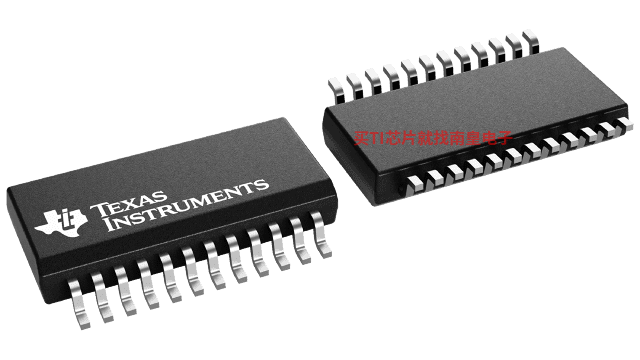
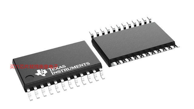
SN74CBT3384CDBQR,工作温度:-40 to 85,封装:SSOP (DBQ)-24,包装数量MPQ:2500个,MSL 等级/回流焊峰值温度:Level-2-260C-1 YEAR,引脚镀层/焊球材料:NIPDAU,TI官网SN74CBT3384CDBQR的批量USD价格:.231(1000+)
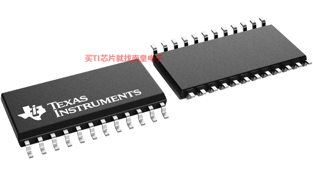
SN74CBT3384CDGVR,工作温度:-40 to 85,封装:TVSOP (DGV)-24,包装数量MPQ:2000个,MSL 等级/回流焊峰值温度:Level-1-260C-UNLIM,引脚镀层/焊球材料:NIPDAU,TI官网SN74CBT3384CDGVR的批量USD价格:.178(1000+)
SN74CBT3384CDWR,工作温度:-40 to 85,封装:SOIC (DW)-24,包装数量MPQ:2000个,MSL 等级/回流焊峰值温度:Level-1-260C-UNLIM,引脚镀层/焊球材料:NIPDAU,TI官网SN74CBT3384CDWR的批量USD价格:.205(1000+)
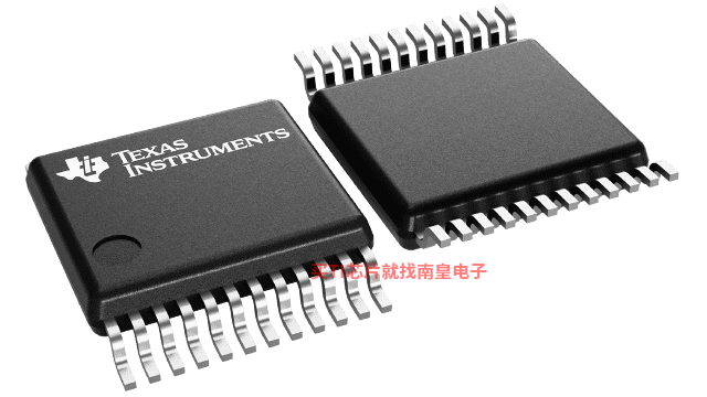
SN74CBT3384CPW,工作温度:-40 to 85,封装:TSSOP (PW)-24,包装数量MPQ:60个,MSL 等级/回流焊峰值温度:Level-1-260C-UNLIM,引脚镀层/焊球材料:NIPDAU,TI官网SN74CBT3384CPW的批量USD价格:.378(1000+)
SN74CBT3384CPWR,工作温度:-40 to 85,封装:TSSOP (PW)-24,包装数量MPQ:2000个,MSL 等级/回流焊峰值温度:Level-1-260C-UNLIM,引脚镀层/焊球材料:NIPDAU,TI官网SN74CBT3384CPWR的批量USD价格:.178(1000+)

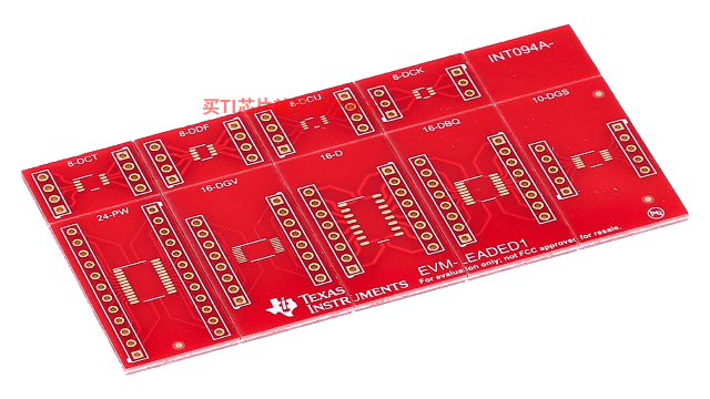
LEADED-ADAPTER1 — 用于快速测试 TI 5、8、10、16 和 24 引脚引线式封装的表面贴装转 DIP 接头适配器
EVM-LEADED1 板可对 TI 的常见引线式封装进行快速测试和电路板试验。该评估板具有足够的空间,可将 TI 的 D、DBQ、DCT、DCU、DDF、DGS、DGV 和 PW 表面贴装封装转换为 100mil DIP 接头。