- ÖÆÔìł§ÉÌŁșTI
- ČúÆ·Àà±đŁșżȘčŰÓë¶à·žŽÓĂÆś
- ŒŒÊőÀàÄżŁșÄŁÄâżȘčŰșͶà·žŽÓĂÆś
- čŠÄÜĂèÊöŁșŸßÓĐšC2V ϳ汣»€șÍ”çÆœŚȘ»»čŠÄÜ”Ä 5VĄą1:1 (SPST)Ąą2 Íš”ÀŚÜÏßżȘčŰŁš”Í”çÆœÓĐЧŁ©
- ”㻜ŐâÀïŽòżȘŒ°ÏÂÔŰSN74CBTD3306C”ÄŒŒÊőÎÄ””ŚÊÁÏ
- TIŽúÀíÇț”ÀŁŹÌáč©”±ÈŐ·ą»őĄąŃÏžń”ÄÖÊÁż±êŚŒŁŹÂúŚăÄú”ÄÄż±êŒÛžń

The SN74CBTD3306C is a high-speed TTL-compatible FET bus switch with low ON-state resistance (ron), allowing for minimal propagation delay. This device features an integrated diode in series with VCC to provide level shifting for 5-V input down to 3.3-V output levels. Active Undershoot-Protection Circuitry on the A and B ports of the SN74CBTD3306C provides protection for undershoot up to –2 V by sensing an undershoot event and ensuring that the switch remains in the proper OFF state.
The SN74CBTD3306C is organized as two 1-bit bus switches with separate output-enable (1OE\, 2OE\) inputs. It can be used as two 1-bit bus switches or as one 2-bit bus switch. When OE\ is low, the associated 1-bit bus switch is ON, and the A port is connected to the B port, allowing bidirectional data flow between ports. When OE\ is high, the associated 1-bit bus switch is OFF, and a high-impedance state exists between the A and B ports.
This device is fully specified for partial-power-down applications using Ioff. The Ioff feature ensures that damaging current will not backflow through the device when it is powered down.
To ensure the high-impedance state during power up or power down, OE\ should be tied to VCC through a pullup resistor; the minimum value of the resistor is determined by the current-sinking capability of the driver.
- Undershoot Protection for Off-Isolation on A and B Ports Up To šC2 V
- Integrated Diode to VCC Provides 5-V Input Down To 3.3-V Output Level Shift
- Bidirectional Data Flow, With Near-Zero Propagation Delay
- Low ON-State Resistance (ron) Characteristics (ron = 3 Typical)
- Low Input/Output Capacitance Minimizes Loading and Signal Distortion (Cio(OFF) = 5 pF Typical)
- Data and Control Inputs Provide Undershoot Clamp Diodes
- VCC Operating Range From 4.5 V to 5.5 V
- Data I/Os Support 0 to 5-V Signaling Levels (0.8-V, 1.2-V, 1.5-V, 1.8-V, 2.5-V, 3.3-V, 5-V)
- Control Inputs Can be Driven by TTL or 5-V/3.3-V CMOS Outputs
- Ioff Supports Partial-Power-Down Mode Operation
- Latch-Up Performance Exceeds 100 mA Per JESD 78, Class II
- ESD Performance Tested Per JESD 22
- 2000-V Human-Body Model (A114-B, Class II)
- 1000-V Charged-Device Model (C101)
- Supports Both Digital and Analog Applications: USB Interface, Memory Interleaving, Bus Isolation, Low-Distortion Signal Gating
- Configuration
- 1:1 SPST
- Number of channels (#)
- 2
- Power supply voltage - single (V)
- 5
- Protocols
- Analog
- Ron (Typ) (Ohms)
- 3
- CON (Typ) (pF)
- 12.5
- Bandwidth (MHz)
- 20
- Operating temperature range (C)
- -40 to 85
- Features
- Undershoot protection
- Input/output continuous current (Max) (mA)
- 128
- Rating
- Catalog
SN74CBTD3306C”ÄÍêŐûĐÍșĆÓĐŁșSN74CBTD3306CDĄąSN74CBTD3306CDRĄąSN74CBTD3306CPWĄąSN74CBTD3306CPWRĄąSN74CBTD3306CPWRG4ŁŹÒÔÏÂÊÇŐâĐ©ČúÆ·”ÄčŰŒüČÎÊęŒ°čÙÍűČÉčș±šŒÛŁș
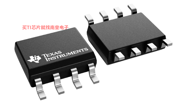
SN74CBTD3306CDŁŹč€ŚśÎÂ¶ÈŁș-40 to 85ŁŹ·âŚ°ŁșSOIC (D)-8ŁŹ°üŚ°ÊęÁżMPQŁș75žöŁŹMSL ”ÈŒ¶/»ŰÁśșž·ćÖ”ÎÂ¶ÈŁșLevel-1-260C-UNLIMŁŹÒęœĆ¶ÆČă/șžÇòČÄÁÏŁșNIPDAUŁŹTIčÙÍűSN74CBTD3306CD”ÄĆúÁżUSDŒÛžńŁș.325Łš1000+Ł©
SN74CBTD3306CDRŁŹč€ŚśÎÂ¶ÈŁș-40 to 85ŁŹ·âŚ°ŁșSOIC (D)-8ŁŹ°üŚ°ÊęÁżMPQŁș2500žöŁŹMSL ”ÈŒ¶/»ŰÁśșž·ćÖ”ÎÂ¶ÈŁșLevel-1-260C-UNLIMŁŹÒęœĆ¶ÆČă/șžÇòČÄÁÏŁșNIPDAUŁŹTIčÙÍűSN74CBTD3306CDR”ÄĆúÁżUSDŒÛžńŁș.125Łš1000+Ł©
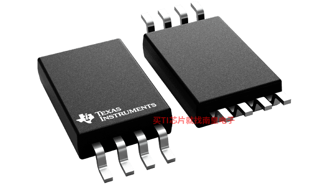
SN74CBTD3306CPWŁŹč€ŚśÎÂ¶ÈŁș-40 to 85ŁŹ·âŚ°ŁșTSSOP (PW)-8ŁŹ°üŚ°ÊęÁżMPQŁș150žöŁŹMSL ”ÈŒ¶/»ŰÁśșž·ćÖ”ÎÂ¶ÈŁșLevel-1-260C-UNLIMŁŹÒęœĆ¶ÆČă/șžÇòČÄÁÏŁșNIPDAUŁŹTIčÙÍűSN74CBTD3306CPW”ÄĆúÁżUSDŒÛžńŁș.325Łš1000+Ł©
SN74CBTD3306CPWRŁŹč€ŚśÎÂ¶ÈŁș-40 to 85ŁŹ·âŚ°ŁșTSSOP (PW)-8ŁŹ°üŚ°ÊęÁżMPQŁș2000žöŁŹMSL ”ÈŒ¶/»ŰÁśșž·ćÖ”ÎÂ¶ÈŁșLevel-1-260C-UNLIMŁŹÒęœĆ¶ÆČă/șžÇòČÄÁÏŁșSNŁŹTIčÙÍűSN74CBTD3306CPWR”ÄĆúÁżUSDŒÛžńŁș.125Łš1000+Ł©
SN74CBTD3306CPWRG4ŁŹč€ŚśÎÂ¶ÈŁș-40 to 85ŁŹ·âŚ°ŁșTSSOP (PW)-8ŁŹ°üŚ°ÊęÁżMPQŁș2000žöŁŹMSL ”ÈŒ¶/»ŰÁśșž·ćÖ”ÎÂ¶ÈŁșLevel-1-260C-UNLIMŁŹÒęœĆ¶ÆČă/șžÇòČÄÁÏŁșNIPDAUŁŹTIčÙÍűSN74CBTD3306CPWRG4”ÄĆúÁżUSDŒÛžńŁș.144Łš1000+Ł©

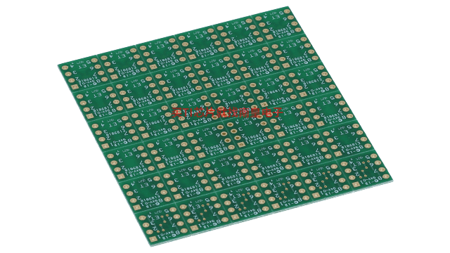
DIP-ADAPTER-EVM ĄȘ DIP ÊÊĆäÆśÆÀčÀÄŁżé
œèÖú DIP-Adapter-EVM ŒÓżìÔËËă·ĆŽóÆś”ÄÔĐÍÉèŒÆșÍČâÊÔŁŹžĂ EVM ÓĐÖúÓÚżìËÙÇáËÉ”ŰÁŹœÓĐĄĐͱíĂæÌùŚ° IC ČąÇҌ۞ń”ÍÁźĄŁÄúżÉÒÔÊčÓĂËæžœ”Ä Samtec ¶ËŚÓ°ćÁŹœÓÈÎșÎÊÜÖ§łÖ”ÄÔËËă·ĆŽóÆśŁŹ»òŐßœ«ŐâĐ©¶ËŚÓ°ćÖ±œÓÁŹœÓÖÁÏÖÓД緥Ł
DIP-Adapter-EVM ÌŚŒțÖ§łÖÁùÖÖłŁÓĂ”ÄÒ”œçÍšÓ÷⌰ŁŹ°üÀšŁș
- D șÍ U (SOIC-8)
- PW (TSSOP-8)
- DGKŁšMSOP-8ĄąVSSOP-8Ł©
- DBVŁšSOT23-6ĄąSOT23-5 șÍ SOT23-3Ł©
- DCKŁšSC70-6 șÍ SC70-5Ł©
- DRL (SOT563-6)
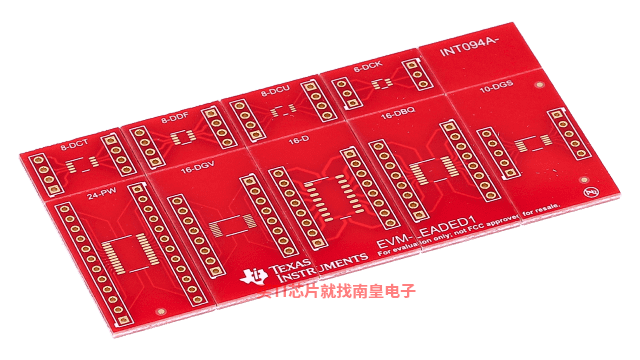
LEADED-ADAPTER1 ĄȘ ÓĂÓÚżìËÙČâÊÔ TI 5Ąą8Ąą10Ąą16 șÍ 24 ÒęœĆÒęÏßÊœ·âŚ°”ıíĂæÌùŚ°ŚȘ DIP œÓÍ·ÊÊĆäÆś
EVM-LEADED1 °ćżÉ¶Ô TI ”ÄłŁŒûÒęÏßÊœ·âŚ°œűĐĐżìËÙČâÊÔș͔緰ćÊÔŃ饣žĂÆÀčÀ°ćŸßÓĐŚăč»”ÄżŐŒäŁŹżÉœ« TI ”Ä DĄąDBQĄąDCTĄąDCUĄąDDFĄąDGSĄąDGV șÍ PW ±íĂæÌùŚ°·âŚ°ŚȘ»»ÎȘ 100mil DIP œÓÍ·ĄŁ


