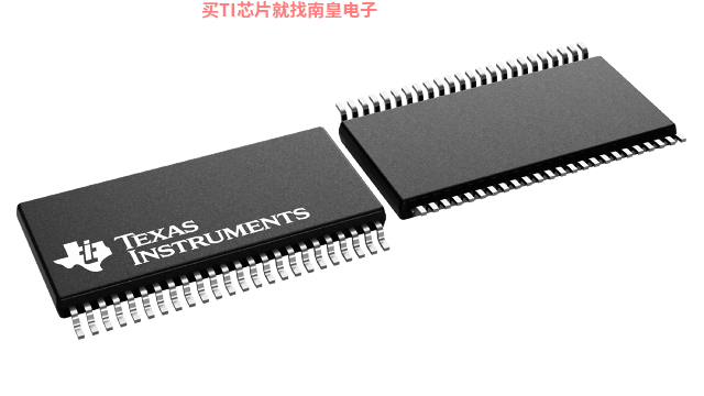
- 制造厂商:TI
- 产品类别:逻辑和电压转换
- 技术类目:电压转换器和电平转换器 - 应用特定的电压转换器
- 功能描述:具有独立 LVTTL 端口和反馈路径的 8 位 LVTTL-GTLP 可调节边沿速率寄存收发器
- 点击这里打开及下载SN74GTLP2033的技术文档资料
- TI代理渠道,提供当日发货、严格的质量标准,满足您的目标价格

The SN74GTLP2033 is a high-drive, 8-bit, three-wire registered transceiver that provides inverted LVTTL-to-GTLP and GTLP-to-LVTTL signal-level translation. The device allows for transparent, latched, and flip-flop modes of data transfer with separate LVTTL input and LVTTL output pins, which provides a feedback path for control and diagnostics monitoring, the same functionality as the SN74FB2033. The device provides a high-speed interface between cards operating at LVTTL logic levels and a backplane operating at GTLP signal levels. High-speed (about three times faster than standard LVTTL or TTL) backplane operation is a direct result of GTLP's reduced output swing (<1 V), reduced input threshold levels, improved differential input, OEC™ circuitry, and TI-OPC™ circuitry. Improved GTLP OEC and TI-OPC circuits minimize bus-settling time and have been designed and tested using several backplane models. The high drive allows incident-wave switching in heavily loaded backplanes with equivalent load impedance down to 11  .
.
GTLP is the Texas Instruments derivative of the Gunning Transceiver Logic (GTL) JEDEC standard JESD 8-3. The ac specification of the SN74GTLP2033 is given only at the preferred higher noise-margin GTLP, but the user has the flexibility of using this device at either GTL (VTT = 1.2 V and VREF = 0.8 V) or GTLP (VTT = 1.5 V and VREF = 1 V) signal levels. For information on using GTLP devices in FB+/BTL applications, refer to TI application reports, Texas Instruments GTLP Frequently Asked Questions, literature number SCEA019, and GTLP in BTL Applications, literature number SCEA017.
Normally, the B port operates at GTLP signal levels. The A-port and control inputs operate at LVTTL logic levels, but are 5-V tolerant and can be directly driven by TTL or 5-V CMOS devices. VREF is the B-port differential input reference voltage.
This device is fully specified for live-insertion applications using Ioff, power-up 3-state, and BIAS VCC. The Ioff circuitry disables the outputs, preventing damaging current backflow through the device when it is powered down. The power-up 3-state circuitry places the outputs in the high-impedance state during power up and power down, which prevents driver conflict. The BIAS VCC circuitry precharges and preconditions the B-port input/output connections, preventing disturbance of active data on the backplane during card insertion or removal, and permits true live-insertion capability.
This GTLP device features TI-OPC circuitry, which actively limits overshoot caused by improperly terminated backplanes, unevenly distributed cards, or empty slots during low-to-high signal transitions. This improves signal integrity, which allows adequate noise margin to be maintained at higher frequencies.
High-drive GTLP backplane interface devices feature adjustable edge-rate control (ERC). Changing the ERC input voltage between low and high adjusts the B-port output rise and fall times.This allows the designer to optimize system data-transfer rate and signal integrity to the backplane load.
When VCC is between 0 and 1.5 V, the device is in the high-impedance state during power up or power down. However, to ensure the high-impedance state above 1.5 V, OEAB\ should be tied to VCC through a pullup resistor and OEAB and OEBA should be tied to GND through a pulldown resistor; the minimum value of the resistor is determined by the current-sinking/current-sourcing capability of the driver.
- Member of the Texas Instruments Widebus? Family
- TI-OPC? Circuitry Limits Ringing on Unevenly Loaded Backplanes
- OEC? Circuitry Improves Signals Integrity and Reduces Electromagnetic Interference
- Bidirectional Interface Between GTLP Signal Levels and LVTTL Logic Levels
- Split LVTTL Port Provides a Feedback Path for Control and Diagnostics Monitoring
- LVTTL Interfaces Are 5-V Tolerant
- High-Drive GTLP Open-Drain Outputs (100 mA)
- LVTTL Outputs (\x9624 mA/24 mA)
- Variable Edge-Rate Control (ERC) Input Selects GTLP Rise and Fall Times for Optimal Data-Transfer Rate and Signal Integrity in Distributed Loads
- Ioff, Power-Up 3-State, and BIAS VCC Support Live Insertion
- Distributed VCC and GND Pins Minimize High-Speed Switching Noise
- Latch-Up Performance Exceeds 100 mA Per JESD 78, Class II
- ESD Protection Exceeds JESD 22
- 2000-V Human-Body Model (A114-A)
- 1000-V Charged-Device Model (C101)
OEC, TI-OPC, and Widebus are trademarks of Texas Instruments.
- Technology Family
- GTLP
- Applications
- GTL
- Rating
- Catalog
- Operating temperature range (C)
- -40 to 85
SN74GTLP2033的完整型号有:SN74GTLP2033DGGR,以下是这些产品的关键参数及官网采购报价:
SN74GTLP2033DGGR,工作温度:-40 to 85,封装:TSSOP (DGG)-48,包装数量MPQ:2000个,MSL 等级/回流焊峰值温度:Level-1-260C-UNLIM,引脚镀层/焊球材料:NIPDAU,TI官网SN74GTLP2033DGGR的批量USD价格:3.416(1000+)

SN74GTLP2033DGGR,工作温度:-40 to 85,封装:TSSOP (DGG)-48,包装数量MPQ:2000个,MSL 等级/回流焊峰值温度:Level-1-260C-UNLIM,引脚镀层/焊球材料:NIPDAU,TI官网SN74GTLP2033DGGR的批量USD价格:3.416(1000+)


