- 制造厂商:TI
- 产品类别:逻辑和电压转换
- 技术类目:触发器、锁存器和寄存器 - D 型触发器
- 功能描述:具有三态输出的 4 位 D 类寄存器
- 点击这里打开及下载SN74LS173A的技术文档资料
- TI代理渠道,提供当日发货、严格的质量标准,满足您的目标价格

The '173 and 'LS173A 4-bit registers include D-type flip-flops featuring totem-pole 3-state outputs capable of driving highly capacitive
or relatively low-impedance loads. The high-impedance third state and increased high-logic-level drive provide these flip-flops with the capability of being connected directly to and driving the bus lines in a bus-organized system without need for interface or pull-up components. Up to 128 of the SN74173 or SN74LS173A outputs can be connected to a common bus and still drive two Series 54/74 or 54LS/74LS TTL normalized loads, respectively. Similarly, up to 49 of the SN54173 or SN54LS173A outputs can be connected to a common bus and drive one additional Series 54/74 or 54LS/74LS TTL normalized load, respectively. To minimize the possibility that two outputs will attempt to take a common bus to opposite logic levels, the output control circuitry is designed so that the average output disable times are shorter than the average output enable times.
Gated enable inputs are provided on these devices for controlling the entry of data into the flip-flops. When both data-enable (G\1, G\2) inputs are low, data at the D inputs are loaded into their respective flip-flops on the next positive transition of the buffered clock input. Gate output-control (M, N) inputs also are provided. When both are low, the normal logic states (high or low levels) of the four outputs are available for driving the loads or bus lines. The outputs are disabled independently from the level of the clock by a high logic level at either output-control input. The outputs then present a high impedance and neither load nor drive the bus line. Detailed operation is given in the function table.
The SN54173 and SN54LS173A are characterized for operation over the full military temperature range of -55°C to 125°C. The SN74173 and SN74LS173A are characterized for operation from 0°C to 70°C.
- 3-State Outputs Interface Directly With System Bus
- Gated Output-Control LInes for Enabling or Disabling the Outputs
- Fully Independent Clock Virtually Eliminates Restrictions for Operating in One of Two Modes:
- Parallel Load
- Do Nothing (Hold)
- For Application as Bus Buffer Registers
- Package Options Include Plastic Small-Outline (D) Packages, Ceramic Flat (W) Packages, Ceramic Chip Carriers (FK), and Standard Plastic (N) and Ceramic (J) DIPs
- Number of channels (#)
- 4
- Technology Family
- LS
- Supply voltage (Min) (V)
- 4.75
- Supply voltage (Max) (V)
- 5.25
- Input type
- Bipolar
- Output type
- 3-State
- Clock Frequency (Max) (MHz)
- 35
- IOL (Max) (mA)
- 24
- IOH (Max) (mA)
- -2.6
- ICC (Max) (uA)
- 24000
- Features
- High speed (tpd 10-50ns)
SN74LS173A的完整型号有:SN74LS173AD、SN74LS173AN,以下是这些产品的关键参数及官网采购报价:
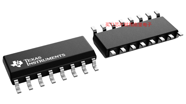
SN74LS173AD,工作温度:0 to 70,封装:SOIC (D)-16,包装数量MPQ:40个,MSL 等级/回流焊峰值温度:Level-1-260C-UNLIM,引脚镀层/焊球材料:NIPDAU,TI官网SN74LS173AD的批量USD价格:.544(1000+)
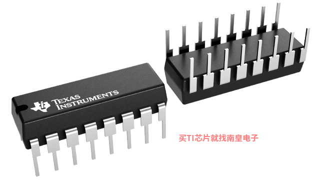
SN74LS173AN,工作温度:0 to 70,封装:PDIP (N)-16,包装数量MPQ:25个,MSL 等级/回流焊峰值温度:N/A for Pkg Type,引脚镀层/焊球材料:NIPDAU,TI官网SN74LS173AN的批量USD价格:.626(1000+)

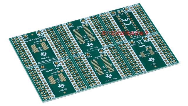
14-24-LOGIC-EVM ― 支持 14 到 24 引脚 PW、DB、D、DW、NS、DYY 和 DGV 封装的通用逻辑 EVM
该 EVM 设计用于支持采用 14 至 24 引脚 D、DW、DB、NS、PW、DYY 或 DGV 封装的任何逻辑器件。


