- 制造厂商:TI
- 产品类别:逻辑和电压转换
- 技术类目:触发器、锁存器和寄存器 - D 型锁存器
- 功能描述:具有三态输出的八路 D 类透明锁存器
- 点击这里打开及下载SN74LS373的技术文档资料
- TI代理渠道,提供当日发货、严格的质量标准,满足您的目标价格

These 8-bit registers feature 3-state outputs designed specifically for driving highly capacitive or relatively low-impedance loads. The high-impedance 3-state and increased high-logic-level drive provide these registers with the capability of being connected directly to and driving the bus lines in a bus-organized system without need for interface or pullup components. These devices are particularly attractive for implementing buffer registers, I/O ports, bidirectional bus drivers, and working registers.
The eight latches of the ’LS373 and ’S373 are transparent D-type latches, meaning that while the enable (C or CLK) input is high, the Q outputs follow the data (D) inputs. When C or CLK is taken low, the output is latched at the level of the data that was set up.
The eight flip-flops of the ’LS374 and ’S374 are edge-triggered D-type flip-flops. On the positive transition of the clock, the Q outputs are set to the logic states that were set up at the D inputs.
Schmitt-trigger buffered inputs at the enable/clock lines of the ’S373 and ’S374 devices simplify system design as ac and dc noise rejection is improved by typically 400 mV due to the input hysteresis. A buffered output-control (OC) input can be used to place the eight outputs in either a normal logic state (high or low logic levels) or the high-impedance state. In the high-impedance state, the outputs neither load nor drive the bus lines significantly.
OC\ does not affect the internal operation of the latches or flip-flops. That is, the old data can be retained or new data can be entered, even while the outputs are off.
- Choice of Eight Latches or Eight D-Type Flip-Flops in a Single Package
- 3-State Bus-Driving Outputs
- Full Parallel Access for Loading
- Buffered Control Inputs
- Clock-Enable Input Has Hysteresis to Improve Noise Rejection (’S373 and ’S374)
- P-N-P Inputs Reduce DC Loading on Data Lines (’S373 and ’S374)
- Number of channels (#)
- 8
- Technology Family
- LS
- Supply voltage (Min) (V)
- 4.75
- Supply voltage (Max) (V)
- 5.25
- Input type
- Bipolar
- Output type
- 3-State
- Clock Frequency (Max) (MHz)
- 35
- IOL (Max) (mA)
- 24
- IOH (Max) (mA)
- -2.6
- ICC (Max) (uA)
- 40000
- Features
- High speed (tpd 10-50ns)
SN74LS373的完整型号有:SN74LS373DW、SN74LS373DWR、SN74LS373N、SN74LS373NSR,以下是这些产品的关键参数及官网采购报价:
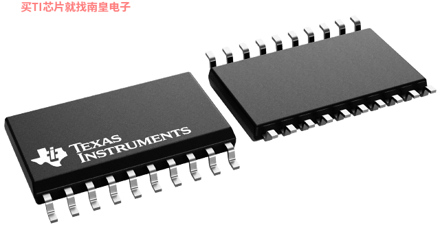
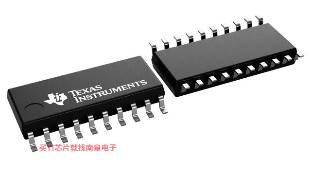
SN74LS373DW,工作温度:0 to 70,封装:SOIC (DW)-20,包装数量MPQ:25个,MSL 等级/回流焊峰值温度:Level-1-260C-UNLIM,引脚镀层/焊球材料:NIPDAU,TI官网SN74LS373DW的批量USD价格:.312(1000+)
SN74LS373DWR,工作温度:0 to 70,封装:SOIC (DW)-20,包装数量MPQ:2000个,MSL 等级/回流焊峰值温度:Level-1-260C-UNLIM,引脚镀层/焊球材料:NIPDAU,TI官网SN74LS373DWR的批量USD价格:.26(1000+)
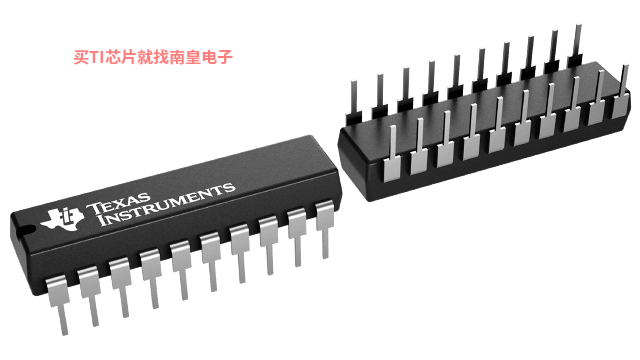
SN74LS373N,工作温度:0 to 70,封装:PDIP (N)-20,包装数量MPQ:20个,MSL 等级/回流焊峰值温度:N/A for Pkg Type,引脚镀层/焊球材料:NIPDAU,TI官网SN74LS373N的批量USD价格:.299(1000+)
SN74LS373NSR,工作温度:0 to 70,封装:SO (NS)-20,包装数量MPQ:2000个,MSL 等级/回流焊峰值温度:Level-1-260C-UNLIM,引脚镀层/焊球材料:NIPDAU,TI官网SN74LS373NSR的批量USD价格:.286(1000+)

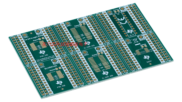
14-24-LOGIC-EVM 支持 14 到 24 引脚 PW、DB、D、DW、NS、DYY 和 DGV 封装的通用逻辑 EVM
该 EVM 设计用于支持采用 14 至 24 引脚 D、DW、DB、NS、PW、DYY 或 DGV 封装的任何逻辑器件。