- 制造厂商:TI
- 产品类别:逻辑和电压转换
- 技术类目:专用逻辑 IC - 数字计时 IC
- 功能描述:压控振荡器
- 点击这里打开及下载SN74LS624的技术文档资料
- TI代理渠道,提供当日发货、严格的质量标准,满足您的目标价格

These voltage-controlled oscillators (VCOs) are improved versions of the original VCO family: SN54LS124, SN54LS324 thru SN54LS327, SN74LS124, and SN74LS324 thru SN74LS327. These new devices feature improved voltage-to-frequency linearity, range, and compensation. With the exception of the 'LS624 and 'LS628, all of these devices feature two independent VCOs in a single monolithic chip. The 'LS624, 'LS625, 'LS626, and 'LS628 have complementary Z outputs. The output frequency for each VCO is established by a single external component (either a capacitor or crystal) in combination with voltage-sensitive inputs used for frequency control and frequency range. Each device has a voltage-sensitive input for frequency control; however, the 'LS624, 'LS628, and 'LS629 devices also have one for frequency range. (See Figures 1 thru 6).
The 'LS628 offers more precise temperature compensation than its 'LS624 counterpart. The 'LS624 features a 600 ohm internal timing resistor. The 'LS628 requires a timing resistor to be connected externally across Rext pins. Temperature compensation will be improved due to the temperature coefficient of the external resistor.
Figure 3 and Figure 6 contain the necessary information to choose the proper capacitor value to obtain the desired operating frequency.
A single 5-volt supply can be used: however, one set of supply voltage and ground pins (VCC and GND) is provided for the enable, synchronization-gating, and output sections, and a separate set (OSC VCC and OSC GND) is provided for the oscillator and associated frequency-control circuits so that effective isolation can be accomplished in the system. For operation of frequencies greater than 10 MHz, it is recommended that two independent supplies be used. Disabling either VCO of the 'LS625 and 'LS625 and 'LS627 can be achieved by removing the appropriate OSC VCC. An enable input is provided on the 'LS624, 'LS626, 'LS628, and 'LS629. When the enable input is low, the output is enabled: when the enable input is high, the internal oscillator is disabled, Y is high, and Z is low. Caution! Crosstalk may occur in the dual devices ('LS625, 'LS626, 'LS627 and 'LS629) when both VCOs are operated simultaneously. To minimize crosstalk, either of the following are recommended: (A) If frequencies are widely separated, use a 10-μh inductor between VCC pins. (B) If frequencies are closely spaced, use two separate VCC supplies or place two series diodes between the VCC pins.
The pulse-synchronization-gating section ensures that the first output pulse is neither clipped nor extended. The duty cycle of the square-wave output is fixed at approximately 50 percent.
The SN54LS624 thru SN54LS629 are characterized for operation over the full military temperature range of -55°C to 125°C. The SN74LS624 thru SN74LS629 are characterized for operation from 0°C to 70°C.
- Separate Supply Voltage Pins for Isolation of Frequency Control Inputs and Oscillators from Output Circuitry
- Highly Stable Operation over Specified Temperature and/or Supply Voltage Ranges
- Technology Family
- LS
- Bits (#)
- 1
- Supply voltage (Min) (V)
- 4.75
- Supply voltage (Max) (V)
- 5.25
- Input type
- Bipolar
- Output type
- Push-Pull
- ICC (Max) (uA)
- 55000
- IOL (Max) (mA)
- 24
- IOH (Max) (mA)
- -1.2
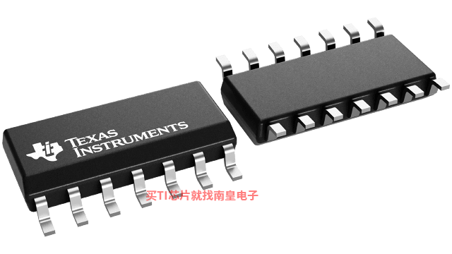
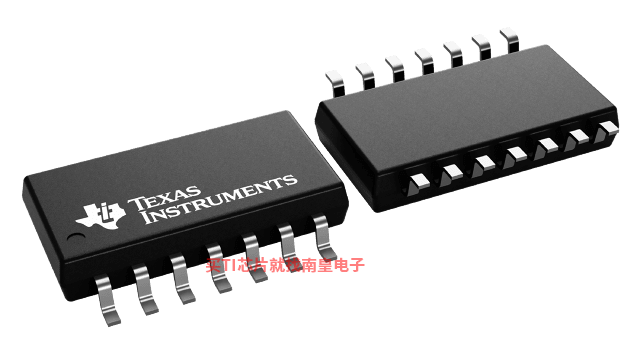
SN74LS624的完整型号有:SN74LS624D、SN74LS624DR、SN74LS624N、SN74LS624NSR,以下是这些产品的关键参数及官网采购报价:
SN74LS624D,工作温度:0 to 70,封装:SOIC (D)-14,包装数量MPQ:50个,MSL 等级/回流焊峰值温度:Level-1-260C-UNLIM,引脚镀层/焊球材料:NIPDAU,TI官网SN74LS624D的批量USD价格:1.553(1000+)
SN74LS624DR,工作温度:0 to 70,封装:SOIC (D)-14,包装数量MPQ:2500个,MSL 等级/回流焊峰值温度:Level-1-260C-UNLIM,引脚镀层/焊球材料:NIPDAU,TI官网SN74LS624DR的批量USD价格:1.294(1000+)
SN74LS624N,工作温度:0 to 70,封装:PDIP (N)-14,包装数量MPQ:25个,MSL 等级/回流焊峰值温度:N/A for Pkg Type,引脚镀层/焊球材料:NIPDAU,TI官网SN74LS624N的批量USD价格:1.488(1000+)
SN74LS624NSR,工作温度:0 to 70,封装:SO (NS)-14,包装数量MPQ:2000个,MSL 等级/回流焊峰值温度:Level-1-260C-UNLIM,引脚镀层/焊球材料:NIPDAU,TI官网SN74LS624NSR的批量USD价格:1.488(1000+)

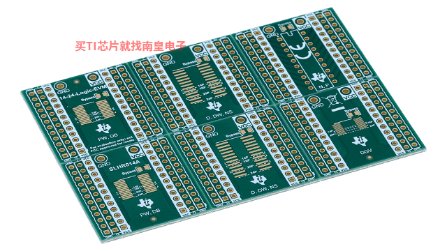
14-24-LOGIC-EVM ― 支持 14 到 24 引脚 PW、DB、D、DW、NS、DYY 和 DGV 封装的通用逻辑 EVM
该 EVM 设计用于支持采用 14 至 24 引脚 D、DW、DB、NS、PW、DYY 或 DGV 封装的任何逻辑器件。


