- 制造厂商:TI
- 产品类别:逻辑和电压转换
- 技术类目:专用逻辑 IC - FIFO 内存 IC
- 功能描述:具有三态输出的 4 x 4 寄存器文件
- 点击这里打开及下载SN74LS670的技术文档资料
- TI代理渠道,提供当日发货、严格的质量标准,满足您的目标价格

The SN54LS670 and SN74LS670 MSI 16-bit TTL register files incorporate the equivalent of 98 gates. The register file is organized as 4 words of 4 bits each and separate on-chip decoding is provided for addressing the four word locations to either write-in or retrieve data. This permits simultaneous writing into one location and reading from another word location.
Four data inputs are available which are used to supply the 4-bit word to be stored. Location of the word is determined by the write-address inputs A and B in conjunction with a write-enable signal. Data applied at the inputs should be in its true form. That is, if a high-level signal is desired from the output, a high-level is applied at the data input for that particular bit location. The latch inputs are arranged so that new data will be accepted only if both internal address gate inputs are high. When this condition exists, data at the D input is transferred to the latch output. When the write-enable input, G\W, is high, the data inputs are inhibited and their levels can cause no change in the information stored in the internal latches. When the read-enable input, G\R, is high, the data outputs are inhibited and go into the high-impedance state.
The individual address lines permit direct acquisition of data stored in any four of the latches. Four individual decoding gates are used to complete the address for reading a word. When the read address is made in conjunction with the read-enable signal, the word appears at the four outputs.
This arrangement — data-entry addressing separate from data-read addressing and individual sense line — eliminates recovery times, permits simultaneous reading and writing, and is limited in speed only by the write time (27 nanoseconds typical) and the read time (24 nanoseconds typical). The register file has a nondestructive readout in that data is not lost when addressed.
All inputs except read enable and write enable are buffered to lower the drive requirements to one Series 54LS/74LS standard load, and input-clamping diodes minimize switching transients to simplify system design. High-speed, double-ended AND-OR-INVERT gates are employed for the read-address function and have high-sink-current, three-state outputs. Up to 128 of these outputs may be bus connected for increasing the capacity up to 512 words. Any number of these registers may be paralleled to provide n-bit word length.
The SN54LS670 is characterized for operation over the full military temperature range of -55°C to 125°C; the SN74LS670 is characterized for operation from 0°C to 70°C.
- Separate Read/Write Addressing Permits Simultaneous Reading and Writing
- Fast Access Times…Typically 20 ns
- Organized as 4 Words of 4 Bits
- Expandable to 512 Words of n-Bits
- For Use as:
- Scratch-Pad Memory
- Buffer Storage between Processors
- Bit Storage in Fast Multiplication Designs
- 3-State Outputs
- SN54LS170 and SN74LS170 Are Similar But Have Open-Collector Outputs
- Supply voltage (Min) (V)
- 4.75
- Supply voltage (Max) (V)
- 5.25
- Input type
- Bipolar
- Output type
- 3-State
- Clock Frequency (Max) (MHz)
- 35
- Features
- Unidirectional
SN74LS670的完整型号有:SN74LS670D、SN74LS670N、SN74LS670NSR,以下是这些产品的关键参数及官网采购报价:
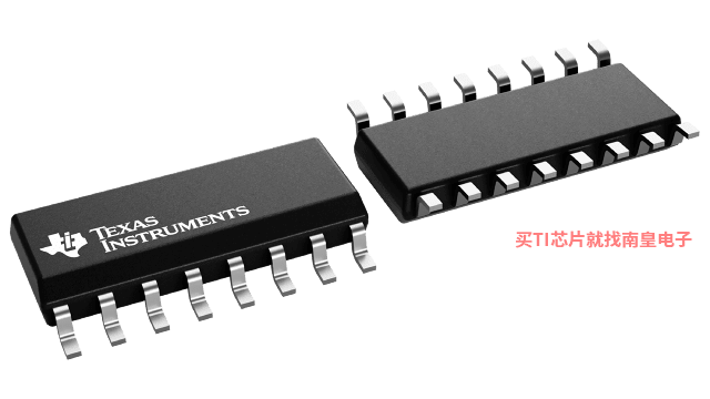
SN74LS670D,工作温度:0 to 70,封装:SOIC (D)-16,包装数量MPQ:40个,MSL 等级/回流焊峰值温度:Level-1-260C-UNLIM,引脚镀层/焊球材料:NIPDAU,TI官网SN74LS670D的批量USD价格:.897(1000+)
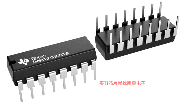
SN74LS670N,工作温度:0 to 70,封装:PDIP (N)-16,包装数量MPQ:25个,MSL 等级/回流焊峰值温度:N/A for Pkg Type,引脚镀层/焊球材料:NIPDAU,TI官网SN74LS670N的批量USD价格:1.032(1000+)
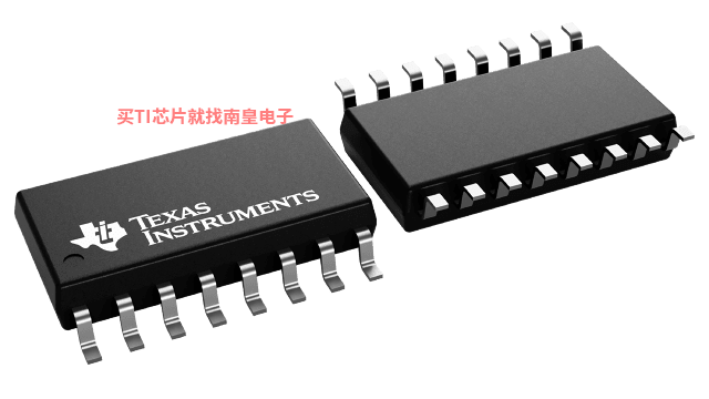
SN74LS670NSR,工作温度:0 to 70,封装:SO (NS)-16,包装数量MPQ:2000个,MSL 等级/回流焊峰值温度:Level-1-260C-UNLIM,引脚镀层/焊球材料:NIPDAU,TI官网SN74LS670NSR的批量USD价格:.897(1000+)

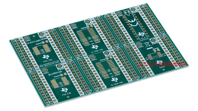
14-24-LOGIC-EVM ― 支持 14 到 24 引脚 PW、DB、D、DW、NS、DYY 和 DGV 封装的通用逻辑 EVM
该 EVM 设计用于支持采用 14 至 24 引脚 D、DW、DB、NS、PW、DYY 或 DGV 封装的任何逻辑器件。