- 制造厂商:TI
- 产品类别:逻辑和电压转换
- 技术类目:专用逻辑 IC - 单稳多谐振荡器(单稳态)
- 功能描述:双路单稳态多谐振荡器
- 点击这里打开及下载SN74LV221A的技术文档资料
- TI代理渠道,提供当日发货、严格的质量标准,满足您的目标价格

The ’LV221A devices are dual multivibrators designed for 2-V to 5.5-V VCC operation. Each multivibrator has a negative-transition-triggered (A\) input and a positive-transition-triggered (B) input, either of which can be used as an inhibit input.
These edge-triggered multivibrators feature output pulse-duration control by three methods. In the first method, the A\ input is low and the B input goes high. In the second method, the B input is high and the A\ input goes low. In the third method, the A\ input is low, the B input is high, and the clear (CLR\) input goes high.
The output pulse duration is programmable by selecting external resistance and capacitance values. The external timing capacitor must be connected between Cext and Rext/Cext (positive) and an external resistor connected between Rext/Cext and VCC. To obtain variable pulse durations, connect an external variable resistor between Rext/Cext and VCC. The output pulse duration also can be reduced by taking CLR\ low.
Pulse triggering occurs at a particular voltage level and is not related directly to the transition time of the input pulse. The A\, B, and CLR\ inputs have Schmitt triggers with sufficient hysteresis to handle slow input transition rates with jitter-free triggering at the outputs.
Once triggered, the outputs are independent of further transitions of the A\ and B inputs and are a function of the timing components, or the output pulses can be terminated by the overriding clear. Input pulses can be of any duration relative to the output pulse. Output pulse duration can be varied by choosing the appropriate timing components. Output rise and fall times are TTL compatible and independent of pulse duration. Typical triggering and clearing sequences are illustrated in the input/output timing diagram.
The variance in output pulse duration from device to device typically is less than ±0.5% for given external timing components. An example of this distribution for the ’LV221A is shown in Figure 8. Variations in output pulse duration versus supply voltage and temperature are shown in Figure 5.
During power up, Q outputs are in the low state, and Q\ outputs are in the high state. The outputs are glitch free, without applying a reset pulse.
These devices are fully specified for partial-power-down applications using Ioff. The Ioff circuitry disables the outputs, preventing damaging current backflow through the devices when they are powered down.
Pin assignments are identical to those of the ’AHC123A and ’AHCT123A devices, so the ’LV221A can be substituted for those devices not using the retrigger feature.
For additional application information on multivibrators, see the application report Designing With The SN74AHC123A and SN74AHCT123A, literature number SCLA014.
- 2-V to 5.5-V VCC Operation
- Max tpd of 11 ns at 5 V
- Support Mixed-Mode Voltage Operation on All Ports
- Schmitt-Trigger Circuitry on A\, B, and CLR\ Inputs for Slow Input Transition Rates
- Overriding Clear Terminates Output Pulse
- Glitch-Free Power-Up Reset on Outputs
- Ioff Supports Partial-Power-Down Mode Operation
- Latch-Up Performance Exceeds 100 mA Per JESD 78, Class II
- ESD Protection Exceeds JESD 22
- 2000-V Human-Body Model (A114-A)
- 200-V Machine Model (A115-A)
- 1000-V Charged-Device Model (C101)
- Number of channels (#)
- 2
- Supply voltage (Min) (V)
- 2
- Supply voltage (Max) (V)
- 5.5
- Technology Family
- LV-A
- Input type
- Schmitt-Trigger
- Output type
- Push-Pull
- ICC (uA)
- 20
- IOL (Max) (mA)
- 12
- IOH (Max) (mA)
- -12
- Features
- Balanced outputs, High speed (tpd 10-50ns), Over-voltage tolerant inputs, Partial power down (Ioff)
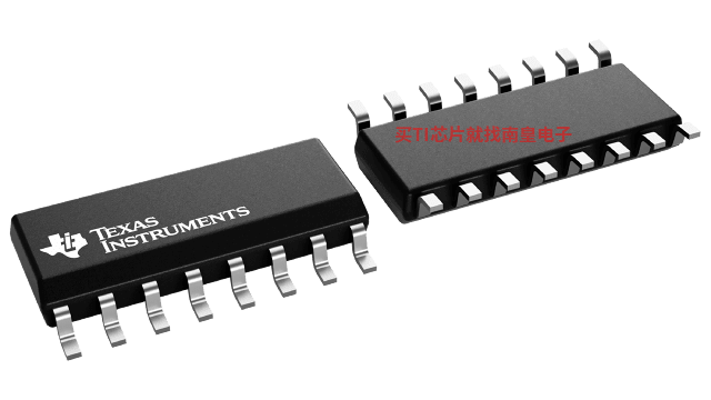
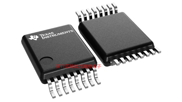
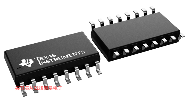
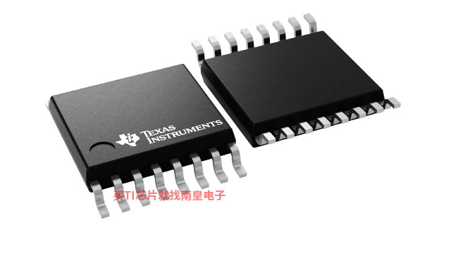
SN74LV221A的完整型号有:SN74LV221AD、SN74LV221ADGVR、SN74LV221ADR、SN74LV221ANSR、SN74LV221APW、SN74LV221APWR、SN74LV221APWT,以下是这些产品的关键参数及官网采购报价:
SN74LV221AD,工作温度:-40 to 85,封装:SOIC (D)-16,包装数量MPQ:40个,MSL 等级/回流焊峰值温度:Level-1-260C-UNLIM,引脚镀层/焊球材料:NIPDAU,TI官网SN74LV221AD的批量USD价格:.51(1000+)
SN74LV221ADGVR,工作温度:-40 to 85,封装:TVSOP (DGV)-16,包装数量MPQ:2000个,MSL 等级/回流焊峰值温度:Level-1-260C-UNLIM,引脚镀层/焊球材料:NIPDAU,TI官网SN74LV221ADGVR的批量USD价格:.425(1000+)
SN74LV221ADR,工作温度:-40 to 85,封装:SOIC (D)-16,包装数量MPQ:2500个,MSL 等级/回流焊峰值温度:Level-1-260C-UNLIM,引脚镀层/焊球材料:NIPDAU,TI官网SN74LV221ADR的批量USD价格:.425(1000+)
SN74LV221ANSR,工作温度:-40 to 85,封装:SO (NS)-16,包装数量MPQ:2000个,MSL 等级/回流焊峰值温度:Level-1-260C-UNLIM,引脚镀层/焊球材料:NIPDAU,TI官网SN74LV221ANSR的批量USD价格:.468(1000+)
SN74LV221APW,工作温度:-40 to 85,封装:TSSOP (PW)-16,包装数量MPQ:90个,MSL 等级/回流焊峰值温度:Level-1-260C-UNLIM,引脚镀层/焊球材料:NIPDAU,TI官网SN74LV221APW的批量USD价格:.51(1000+)
SN74LV221APWR,工作温度:-40 to 85,封装:TSSOP (PW)-16,包装数量MPQ:2000个,MSL 等级/回流焊峰值温度:Level-1-260C-UNLIM,引脚镀层/焊球材料:NIPDAU,TI官网SN74LV221APWR的批量USD价格:.425(1000+)
SN74LV221APWT,工作温度:-40 to 85,封装:TSSOP (PW)-16,包装数量MPQ:250个,MSL 等级/回流焊峰值温度:Level-1-260C-UNLIM,引脚镀层/焊球材料:NIPDAU,TI官网SN74LV221APWT的批量USD价格:.51(1000+)

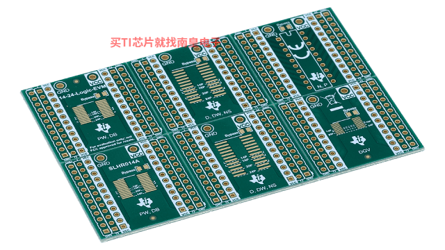
14-24-LOGIC-EVM ― 支持 14 到 24 引脚 PW、DB、D、DW、NS、DYY 和 DGV 封装的通用逻辑 EVM
该 EVM 设计用于支持采用 14 至 24 引脚 D、DW、DB、NS、PW、DYY 或 DGV 封装的任何逻辑器件。
