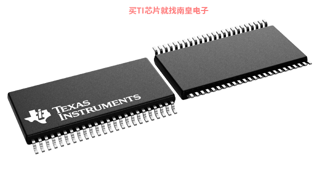
- 制造厂商:TI
- 产品类别:逻辑和电压转换
- 技术类目:缓冲器、驱动器和收发器 - 同相缓冲器和驱动器
- 功能描述:具有三态输出的增强型产品 16 通道、1.65V 至 3.6V 缓冲器
- 点击这里打开及下载SN74LVC16244A-EP的技术文档资料
- TI代理渠道,提供当日发货、严格的质量标准,满足您的目标价格

This 16-bit buffer/driver is designed for 1.65-V to 3.6-V VCC operation.
The SN74LVC16244A is designed specifically to improve the performance and density of 3-state memory address drivers, clock drivers, and bus-oriented receivers and transmitters.
The device can be used as four 4-bit buffers, two 8-bit buffers, or one 16-bit buffer. It provides true outputs and symmetrical active-low output-enable (OE)\ inputs.
Inputs can be driven from either 3.3-V or 5-V devices. This feature allows the use of this device as a translator in a mixed 3.3-V/5-V system environment.
This device is fully specified for partial-power-down applications using Ioff. The Ioff circuitry disables the outputs, preventing damaging current backflow through the device when it is powered down.
To ensure the high-impedance state during power up or power down, OE\ should be tied to VCC through a pullup resistor; the minimum value of the resistor is determined by the current-sinking capability of the driver.
- Controlled Baseline
- One Assembly/Test Site, One Fabrication Site
- Enhanced Diminishing Manufacturing Sources (DMS) Support
- Enhanced Product-Change Notification
- Qualification Pedigree
- Member of the Texas Instruments Widebus? Family
- Operates From 1.65 V to 3.6 V
- Inputs Accept Voltages to 5.5 V
- Max tpd of 4.1 ns at 3.3 V
- Typical VOLP (Output Ground Bounce) <0.8 V at VCC = 3.3 V, TA = 25°C
- Typical VOHV (Output VOH Undershoot) >2 V at VCC = 3.3 V, TA = 25°C
- Ioff Supports Partial-Power-Down Mode Operation
- Supports Mixed-Mode Signal Operation On All Ports (5-V Input/Output Voltage With 3.3-V VCC)
- Latch-Up Performance Exceeds 250 mA Per JESD 17
- ESD Protection Exceeds JESD 22
- 2000-V Human-Body Model (A114-A)
- 1000-V Charged-Device Model (C101)
Component qualification in accordance with JEDEC and industry standards to ensure reliable operation over an extended temperature range. This includes, but is not limited to, Highly Accelerated Stress Test (HAST) or biased 85/85, temperature cycle, autoclave or unbiased HAST, electromigration, bond intermetallic life, and mold compound life. Such qualification testing should not be viewed as justifying use of this component beyond specified performance and environmental limits. Widebus is a trademark of Texas Instruments.
- Technology Family
- LVC
- Supply voltage (Min) (V)
- 1.65
- Supply voltage (Max) (V)
- 3.6
- Number of channels (#)
- 16
- IOL (Max) (mA)
- 24
- ICC (Max) (uA)
- 20
- IOH (Max) (mA)
- -24
- Input type
- Standard CMOS
- Output type
- 3-State
- Features
- Balanced outputs, Very high speed (tpd 5-10ns), Partial power down (Ioff), Over-voltage tolerant inputs
- Rating
- HiRel Enhanced Product
SN74LVC16244A-EP的完整型号有:CLVC16244AIDGGREP、V62/04724-01XE,以下是这些产品的关键参数及官网采购报价:
CLVC16244AIDGGREP,工作温度:-40 to 85,封装:TSSOP (DGG)-48,包装数量MPQ:2000个,MSL 等级/回流焊峰值温度:Level-1-260C-UNLIM,引脚镀层/焊球材料:NIPDAU,TI官网CLVC16244AIDGGREP的批量USD价格:1.442(1000+)
V62/04724-01XE,工作温度:-40 to 85,封装:TSSOP (DGG)-48,包装数量MPQ:2000个,MSL 等级/回流焊峰值温度:Level-1-260C-UNLIM,引脚镀层/焊球材料:NIPDAU,TI官网V62/04724-01XE的批量USD价格:1.442(1000+)


