- 制造厂商:TI
- 产品类别:逻辑和电压转换
- 技术类目:触发器、锁存器和寄存器 - D 型触发器
- 功能描述:具有三态输出的汽车类单路 D 类触发器
- 点击这里打开及下载SN74LVC1G374-Q1的技术文档资料
- TI代理渠道,提供当日发货、严格的质量标准,满足您的目标价格

This single D-type flip-flop is designed for 1.65-V to 5.5-V VCC operation.
The SN74LVC1G374 features a 3-state output designed specifically for driving highly capacitive or relatively low-impedance loads. This device is particularly suitable for implementing buffer registers, input/output (I/O) ports, bidirectional bus drivers, and working registers.
On the positive transition of the clock (CLK) input, the Q output is set to the logic level set up at the data (D) input.
A buffered output-enable (OE) input can be used to place the output in either a normal logic state (high or low logic levels) or the high-impedance state. In the high-impedance state, the output neither loads nor drives the bus lines significantly. The high-impedance state and increased drive provide the capability to drive bus lines without interface or pullup components.
OE does not affect the internal operations of the flip-flop. Old data can be retained or new data can be entered while the outputs are in the high-impedance state.
To ensure the high-impedance state during power up or power down, OE should be tied to VCC through a pullup resistor; the minimum value of the resistor is determined by the current-sinking capability of the driver.
To ensure the high-impedance state during power up or power down, OE should be tied to VCC through a pullup resistor; the minimum value of the resistor is determined by the current-sinking capability of the driver.
This device is fully specified for partial-power-down applications using Ioff. The Ioff circuitry disables the outputs, preventing damaging current backflow through the device when it is powered down.
- Qualified for Automotive Applications
- Supports 5-V VCC Operation
- Inputs Accept Voltages to 5.5 V
- Max tpd of 4 ns at 3.3 V
- Low Power Consumption, 10-μA Max ICC
- ±24-mA Output Drive at 3.3 V
- Ioff Supports Partial-Power-Down Mode Operation
- Latch-Up Performance Exceeds 100 mA Per JESD 78, Class II
- ESD Protection Exceeds JESD 22
- 2000-V Human-Body Model (A114-A)
- 200-V Machine Model (A115-A)
- 1000-V Charged-Device Model (C101)
- Number of channels (#)
- 1
- Technology Family
- LVC
- Supply voltage (Min) (V)
- 1.65
- Supply voltage (Max) (V)
- 5.5
- Input type
- Standard CMOS
- Output type
- 3-State
- Clock Frequency (Max) (MHz)
- 150
- IOL (Max) (mA)
- 32
- IOH (Max) (mA)
- -32
- ICC (Max) (uA)
- 10
- Features
- Balanced outputs, Very high speed (tpd 5-10ns), Over-voltage tolerant inputs, Partial power down (Ioff)
SN74LVC1G374-Q1的完整型号有:CLVC1G374QDBVRQ1、CLVC1G374QDCKRQ1,以下是这些产品的关键参数及官网采购报价:
CLVC1G374QDBVRQ1,工作温度:-40 to 125,封装:SOT-23 (DBV)-6,包装数量MPQ:3000个,MSL 等级/回流焊峰值温度:Level-1-260C-UNLIM,引脚镀层/焊球材料:NIPDAU,TI官网CLVC1G374QDBVRQ1的批量USD价格:.083(1000+)
CLVC1G374QDCKRQ1,工作温度:-40 to 125,封装:SC70 (DCK)-6,包装数量MPQ:3000个,MSL 等级/回流焊峰值温度:Level-1-260C-UNLIM,引脚镀层/焊球材料:NIPDAU,TI官网CLVC1G374QDCKRQ1的批量USD价格:.083(1000+)

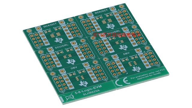
5-8-LOGIC-EVM ― 支持 5 至 8 引脚 DCK、DCT、DCU、DRL 和 DBV 封装的通用逻辑 EVM
灵活的 EVM 设计用于支持具有 5 至 8 引脚数且采用 DCK、DCT、DCU、DRL 或 DBV 封装的任何器件。TIDA-00580 ― 汽车级 16 位旋转正交解码器参考设计
人们在许多情况下都喜欢通过触摸屏使用旋钮。该解决方案最大程度减少了为了监测旋转正交编码器的旋转方向和距离而需要与微处理器进行的连接。