- 制造厂商:TI
- 产品类别:逻辑和电压转换
- 技术类目:缓冲器、驱动器和收发器 - 通用收发器
- 功能描述:具有三态输出的八路总线收发器和寄存器
- 点击这里打开及下载SN74LVC2952A的技术文档资料
- TI代理渠道,提供当日发货、严格的质量标准,满足您的目标价格

This octal bus transceiver and register is designed for 1.65-V to 3.6-V VCC operation.
The SN74LVC2952A consists of two 8-bit back-to-back registers that store data flowing in both directions between two bidirectional buses. Data on the A or B bus is stored in the registers on the low-to-high transition of the clock (CLKAB or CLKBA) input, provided that the clock-enable (CLKENAB\ or CLKENBA)\ input is low. Taking the output-enable (OEAB\ or OEBA)\ input low accesses the data on either port.
Inputs can be driven from either 3.3-V or 5-V devices. This feature allows the use of these devices as translators in a mixed 3.3-V/5-V system environment.
To ensure the high-impedance state during power up or power down, OE\ should be tied to VCC through a pullup resistor; the minimum value of the resistor is determined by the current-sinking capability of the driver.
This device is fully specified for partial-power-down applications using Ioff. The Ioff circuitry disables the outputs, preventing damaging current backflow through the device when it is powered down.
- Operates From 1.65 V to 3.6 V
- Inputs Accept Voltages to 5.5 V
- Max tpd of 8.2 ns at 3.3 V
- Typical VOLP (Output Ground Bounce) <0.8 V at VCC = 3.3 V, TA = 25°C
- Typical VOHV (Output VOH Undershoot) >2 V at VCC = 3.3 V, TA = 25°C
- Supports Mixed-Mode Signal Operation on All Ports (5-V Input/Output Voltage With 3.3-V VCC)
- Ioff Supports Partial-Power-Down Mode Operation
- Latch-Up Performance Exceeds 250 mA Per JESD 17
- ESD Protection Exceeds JESD 22
- 2000-V Human-Body Model (A114-A)
- 1000-V Charged-Device Model (C101)
- IOL (Max) (mA)
- 24
- IOH (Max) (mA)
- -24
- Technology Family
- LVC
- Rating
- Catalog
- Operating temperature range (C)
- -40 to 85
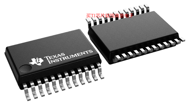
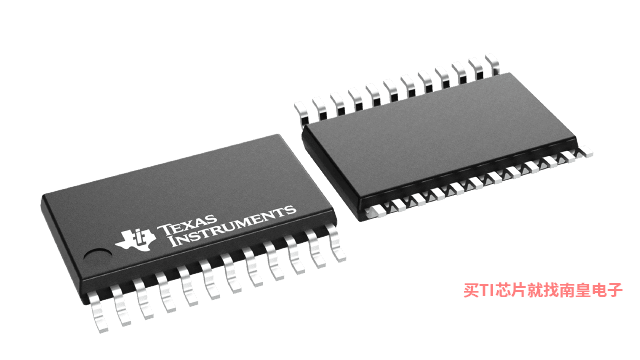
SN74LVC2952A的完整型号有:SN74LVC2952ADBR、SN74LVC2952APWR,以下是这些产品的关键参数及官网采购报价:
SN74LVC2952ADBR,工作温度:-40 to 85,封装:SSOP (DB)-24,包装数量MPQ:2000个,MSL 等级/回流焊峰值温度:Level-1-260C-UNLIM,引脚镀层/焊球材料:NIPDAU,TI官网SN74LVC2952ADBR的批量USD价格:0.419(1000+)
SN74LVC2952APWR,工作温度:-40 to 85,封装:TSSOP (PW)-24,包装数量MPQ:2000个,MSL 等级/回流焊峰值温度:Level-1-260C-UNLIM,引脚镀层/焊球材料:NIPDAU,TI官网SN74LVC2952APWR的批量USD价格:0.381(1000+)

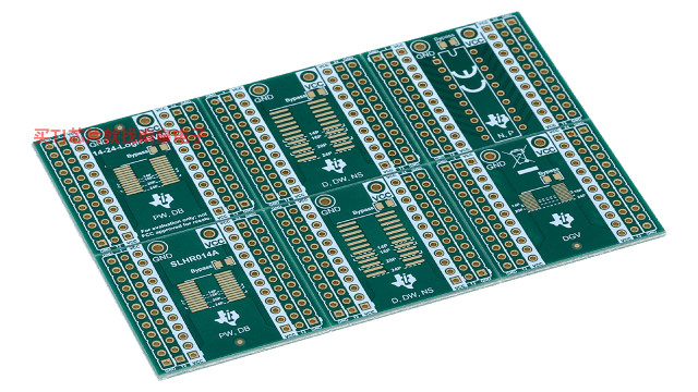
14-24-LOGIC-EVM ― 支持 14 到 24 引脚 PW、DB、D、DW、NS、DYY 和 DGV 封装的通用逻辑 EVM
该 EVM 设计用于支持采用 14 至 24 引脚 D、DW、DB、NS、PW、DYY 或 DGV 封装的任何逻辑器件。