

SN74LVC2GU04-Q1的基本参数
- 制造厂商:TI
- 产品类别:逻辑和电压转换
- 技术类目:缓冲器、驱动器和收发器 - 反向缓冲器和驱动器
- 功能描述:汽车类 2 通道、1.65V 至 5.5V 反相器
- 点击这里打开及下载SN74LVC2GU04-Q1的技术文档资料
- TI代理渠道,提供当日发货、严格的质量标准,满足您的目标价格

SN74LVC2GU04-Q1的产品详情:
This dual inverter is designed for 1.65-V to 5.5-V VCC operation.
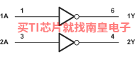
The SN74LVC2GU04-Q1 device contains two inverters with unbuffered outputs and performs the Boolean function Y = A.
SN74LVC2GU04-Q1的优势和特性:
- AEC-Q100 Qualified for automotive applications:
- Device temperature grade 1: –40°C to +125°C, TA
- Supports 5-V VCC operation
- Inputs accept voltages to 5.5 V
- Max tpd of 3.7 ns at 3.3 V
- Low power consumption, 10-μA max ICC
- ±24-mA Output drive at 3.3 V
- Typical VOLP (output ground bounce) <0.8 V at VCC = 3.3 V, TA = 25°C
- Typical VOHV (output VOH undershoot) >2 V at VCC = 3.3 V, TA = 25°C
- Can be used as a down translator to translate inputs from a max of 5.5 V down to the VCC level
- Unbuffered outputs
SN74LVC2GU04-Q1的参数(英文):
- Technology Family
- LVC
- Supply voltage (Min) (V)
- 1.65
- Supply voltage (Max) (V)
- 5.5
- Number of channels (#)
- 2
- IOL (Max) (mA)
- -32
- IOH (Max) (mA)
- -32
- ICC (Max) (uA)
- 10
- Input type
- Standard CMOS
- Output type
- Push-Pull
- Features
- Balanced outputs, Very high speed (tpd 5-10ns), Partial power down (Ioff), Over-voltage tolerant inputs, Unbuffered
- Rating
- Automotive
SN74LVC2GU04-Q1具体的完整产品型号参数及价格(美元):
SN74LVC2GU04-Q1的完整型号有:1P2GU04QDRYRQ1,以下是这些产品的关键参数及官网采购报价:
1P2GU04QDRYRQ1,工作温度:-40 to 125,封装:SON (DRY)-6,包装数量MPQ:5000个,MSL 等级/回流焊峰值温度:Level-1-260C-UNLIM,引脚镀层/焊球材料:NIPDAU,TI官网1P2GU04QDRYRQ1的批量USD价格:.228(1000+)

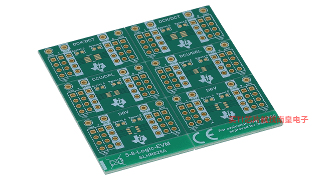
SN74LVC2GU04-Q1的评估套件:
5-8-LOGIC-EVM — 支持 5 至 8 引脚 DCK、DCT、DCU、DRL 和 DBV 封装的通用逻辑 EVM
灵活的 EVM 设计用于支持具有 5 至 8 引脚数且采用 DCK、DCT、DCU、DRL 或 DBV 封装的任何器件。SN74LVC2GU04-Q1的电路图解:
SN74LVC2GU04-Q1的评估套件:
相关型号

丰富的可销售TI代理库存,专业的销售团队可随时响应您的紧急需求,目标成为有价值的TI代理