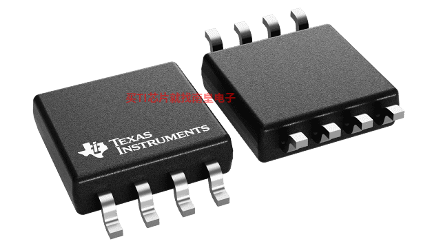
- 制造厂商:TI
- 产品类别:逻辑和电压转换
- 技术类目:电压转换器和电平转换器 - 方向控制型电压转换器
- 功能描述:具有可配置电压转换和三态输出的增强型产品双位双电源收发器
- 点击这里打开及下载SN74LVC2T45-EP的技术文档资料
- TI代理渠道,提供当日发货、严格的质量标准,满足您的目标价格

This dual-bit noninverting bus transceiver uses two separate configurable power-supply rails. The A port is designed to track VCCA. VCCA accepts any supply voltage from 1.65 V to 5.5 V. The B port is designed to track VCCB. VCCB accepts any supply voltage from 1.65 V to 5.5 V. This allows for universal low-voltage bidirectional translation between any of the 1.8-V, 2.5-V, 3.3-V, and 5-V voltage nodes.
The SN74LVC2T45 is designed for asynchronous communication between two data buses. The logic levels of the direction-control (DIR) input activate either the B-port outputs or the A-port outputs. The device transmits data from the A bus to the B bus when the B-port outputs are activated, and from the B bus to the A bus when the A-port outputs are activated. The input circuitry on both A and B ports always is active and must have a logic HIGH or LOW level applied to prevent excess ICC and ICCZ.
The SN74LVC2T45 is designed so that the DIR input circuit is supplied by VCCA.
This device is fully specified for partial-power-down applications using Ioff. The Ioff circuitry disables the outputs, preventing damaging current backflow through the device when it is powered down.
The VCC isolation feature ensures that if either VCC input is at GND, both ports are in the high-impedance state.
NanoFree™ package technology is a major breakthrough in IC packaging concepts, using the die as the package.
- Available in the Texas Instruments NanoFree? Package
- Fully Configurable Dual-Rail Design Allows Each Port to Operate Over the Full 1.65-V to 5.5-V Power-Supply Range
- VCC Isolation Feature – If Either VCC Input Is at GND, Both Ports Are in the High-Impedance State
- DIR Input Circuit Referenced to VCCA
- Low Power Consumption, 10-μA Max ICC
- ±24-mA Output Drive at 3.3 V
- Ioff Supports Partial-Power-Down Mode Operation
- Max Data Rates
- 420 Mbps (3.3-V to 5-V Translation)
- 210 Mbps (Translate to 3.3 V)
- 140 Mbps (Translate to 2.5 V)
- 75 Mbps (Translate to 1.8 V)
- Latch-Up Performance Exceeds 100 mA Per JESD 78, Class II
- ESD Protection Exceeds JESD 22
- 4000-V Human-Body Model (A114-A)
- 200-V Machine Model (A115-A)
- 1000-V Charged-Device Model (C101)
- SUPPORTS DEFENSE, AEROSPACE, AND MEDICAL APPLICATIONS
- Controlled Baseline
- One Assembly/Test Site
- One Fabrication Site
- Available Temperature Ranges:
- –55°C to 125°C
- –55°C to 150°C
- Extended Product Life Cycle
- Extended Product-Change Notification
- Product Traceability
NanoFree Is a trademark of Texas Instruments
- Technology Family
- LVC
- Applications
- GPIO, I2S
- Bits (#)
- 2
- High input voltage (Min) (Vih)
- 1.08
- High input voltage (Max) (Vih)
- 5.5
- Vout (Min) (V)
- 1.65
- Vout (Max) (V)
- 5.5
- IOH (Max) (mA)
- -32
- IOL (Max) (mA)
- 32
- Rating
- HiRel Enhanced Product
SN74LVC2T45-EP的完整型号有:SN74LVC2T45MDCTTEP、V62/09604-01XE,以下是这些产品的关键参数及官网采购报价:
SN74LVC2T45MDCTTEP,工作温度:-55 to 125,封装:SM8 (DCT)-8,包装数量MPQ:250个,MSL 等级/回流焊峰值温度:Level-1-260C-UNLIM,引脚镀层/焊球材料:NIPDAU,TI官网SN74LVC2T45MDCTTEP的批量USD价格:1.053(1000+)
V62/09604-01XE,工作温度:-55 to 125,封装:SM8 (DCT)-8,包装数量MPQ:250个,MSL 等级/回流焊峰值温度:Level-1-260C-UNLIM,引脚镀层/焊球材料:NIPDAU,TI官网V62/09604-01XE的批量USD价格:1.053(1000+)


