- ���쳧�̣�TI
- ��Ʒ������͵�ѹת��
- ������Ŀ�����������������ͼĴ��� - D ��������
- ����������������̬�������ǿ�Ͳ�Ʒ��· D ����������
- ������������SN74LVC573A-EP�ļ����ĵ�����
- TI�����������ṩ���շ������ϸ������������������Ŀ��۸�

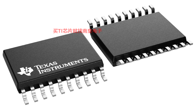
The SN74LVC573A-EP octal transparent D-type latch is designed for 2.7-V to 3.6-V VCC operation.
This device features 3-state outputs designed specifically for driving highly capacitive or relatively low-impedance loads. It is particularly suitable for implementing buffer registers, input/output (I/O) ports, bidirectional bus drivers, and working registers.
While the latch-enable (LE) input is high, the Q outputs follow the data (D) inputs. When LE is taken low, the Q outputs are latched at the logic levels at the D inputs.
A buffered output-enable (OE)\ input can be used to place the eight outputs in either a normal logic state (high or low logic levels) or the high-impedance state. In the high-impedance state, the outputs neither load nor drive the bus lines significantly. The high-impedance state and increased drive provide the capability to drive bus lines without interface or pullup components.
OE\ does not affect the internal operations of the latches. Old data can be retained or new data can be entered while the outputs are in the high-impedance state.
This device is fully specified for partial-power-down applications using Ioff. The Ioff circuitry disables the outputs, preventing damaging current backflow through the device when it is powered down.
To ensure the high-impedance state during power up or power down, OE\ should be tied to VCC through a pullup resistor; the minimum value of the resistor is determined by the current-sinking capability of the driver.
Inputs can be driven from either 3.3-V or 5-V devices. This feature allows the use of this device as a translator in a mixed 3.3-V/5-V system environment.
- Controlled Baseline
- One Assembly/Test Site, One Fabrication Site
- Extended Temperature Performance of �C40��C to 125��C
- Enhanced Diminishing Manufacturing Sources (DMS) Support
- Enhanced Product-Change Notification
- Qualification Pedigree
- Operates From 2 V to 3.6 V
- Inputs Accept Voltages to 5.5 V
- Max tpd of 6.9 ns at 3.3 V
- Typical VOLP (Output Ground Bounce) <0.8 V at VCC = 3.3 V, TA = 25��C
- Typical VOHV (Output VOH Undershoot) >2 V at VCC = 3.3 V, TA = 25��C
- Supports Mixed-Mode Signal Operation on All Ports (5-V Input/Output Voltage With 3.3-V VCC)
- Ioff Supports Partial-Power-Down Mode Operation
Component qualification in accordance with JEDEC and industry standards to ensure reliable operation over an extended temperature range. This includes, but is not limited to, Highly Accelerated Stress Test (HAST) or biased 85/85, temperature cycle, autoclave or unbiased HAST, electromigration, bond intermetallic life, and mold compound life. Such qualification testing should not be viewed as justifying use of this component beyond specified performance and environmental limits.
- Number of channels (#)
- 8
- Technology Family
- LVC
- Supply voltage (Min) (V)
- 2
- Supply voltage (Max) (V)
- 3.6
- Input type
- Standard CMOS
- Output type
- 3-State
- Clock Frequency (Max) (MHz)
- 100
- IOL (Max) (mA)
- 24
- IOH (Max) (mA)
- -24
- ICC (Max) (uA)
- 10
- Features
- Balanced outputs, Very high speed (tpd 5-10ns), Over-voltage tolerant inputs, Partial power down (Ioff), Flow-through pinout
SN74LVC573A-EP�������ͺ��У�SN74LVC573AQPWREP��V62/04667-01YE����������Щ��Ʒ�Ĺؼ������������ɹ����ۣ�
SN74LVC573AQPWREP�������¶ȣ�-40 to 125����װ��TSSOP (PW)-20����װ����MPQ��2000����MSL �ȼ�/��������ֵ�¶ȣ�Level-1-260C-UNLIM�����ŶƲ�/������ϣ�NIPDAU��TI����SN74LVC573AQPWREP������USD�۸�.833��1000+��
V62/04667-01YE�������¶ȣ�-40 to 125����װ��TSSOP (PW)-20����װ����MPQ��2000����MSL �ȼ�/��������ֵ�¶ȣ�Level-1-260C-UNLIM�����ŶƲ�/������ϣ�NIPDAU��TI����V62/04667-01YE������USD�۸�.833��1000+��


