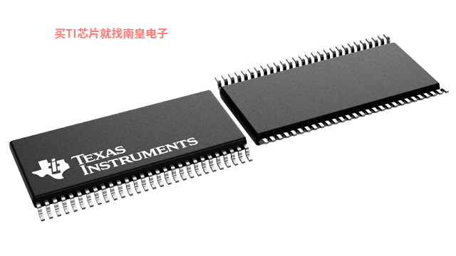
- 制造厂商:TI
- 产品类别:逻辑和电压转换
- 技术类目:缓冲器、驱动器和收发器 - 通用收发器
- 功能描述:具有三态输出的 3.3V ABT 18 位通用总线收发器
- 点击这里打开及下载SN74LVT16501的技术文档资料
- TI代理渠道,提供当日发货、严格的质量标准,满足您的目标价格

The 'LVT16501 are 18-bit universal bus transceivers designed for low-voltage (3.3-V) VCC operation, but with the capability to provide a TTL interface to a 5-V system environment.
Data flow in each direction is controlled by output-enable (OEAB and ![]() ), latch-enable (LEAB and LEBA), and clock (CLKAB and CLKBA) inputs. For A-to-B data flow, the devices operate in the transparent mode when LEAB is high. When LEAB is low, the A data is latched if CLKAB is held at a high or low logic level. If LEAB is low, the A-bus data is stored in the latch/flip-flop on the low-to-high transition of CLKAB. When OEAB is high, the outputs are active. When OEAB is low, the outputs are in the high-impedance state.
), latch-enable (LEAB and LEBA), and clock (CLKAB and CLKBA) inputs. For A-to-B data flow, the devices operate in the transparent mode when LEAB is high. When LEAB is low, the A data is latched if CLKAB is held at a high or low logic level. If LEAB is low, the A-bus data is stored in the latch/flip-flop on the low-to-high transition of CLKAB. When OEAB is high, the outputs are active. When OEAB is low, the outputs are in the high-impedance state.
Data flow for B to A is similar to that of A to B but uses ![]() , LEBA, and CLKBA. The output enables are complementary (OEAB is active high and
, LEBA, and CLKBA. The output enables are complementary (OEAB is active high and ![]() is active low).
is active low).
Active bus-hold circuitry is provided to hold unused or floating data inputs at a valid logic level.
To ensure the high-impedance state during power up or power down, ![]() should be tied to VCC through a pullup resistor. The minimum value of the resistor is determined by the current-sinking capability of the driver. OE should be tied to GND through a pulldown resistor; the minimum value of the resistor is determined by the current-sourcing capability of the driver.
should be tied to VCC through a pullup resistor. The minimum value of the resistor is determined by the current-sinking capability of the driver. OE should be tied to GND through a pulldown resistor; the minimum value of the resistor is determined by the current-sourcing capability of the driver.
The SN74LVT16501 is available in TI's shrink small-outline (DL) and thin shrink small-outline (DGG) packages, which provide twice the input/output (I/O) pin count and functionality of standard small-outline packages in the same printed circuit board area.
The SN54LVT16501 is characterized for operation over the full military temperature range of -55°C to 125°C. The SN74LVT16501 is characterized for operation from -40°C to 85°C.
- State-of-the-Art Advanced BiCMOS Technology (ABT) Design for 3.3-V Operation and Low-Static Power Dissipation
- Members of the Texas Instruments WidebusTM Family
- Support Mixed-Mode Signal Operation (5-V Input and Output Voltages With 3.3-V VCC)
- Support Unregulated Battery Operation Down to 2.7 V
- UBTTM (Universal Bus Transceiver) Combines D-Type Latches and D-Type Flip-Flops for Operation in Transparent, Latched, or Clocked Mode
- Typical VOLP (Output Ground Bounce) < 0.8 V at VCC = 3.3 V, TA = 25°C
- ESD Protection Exceeds 2000 V Per MIL-STD-883, Method 3015; Exceeds 200 V Using Machine Model (C = 200 pF, R = 0)
- Latch-Up Performance Exceeds 500 mA Per JEDEC Standard JESD-17
- Bus Hold on Data Inputs Eliminates the Need for External Pullup/Pulldown Resistors
- Support Live Insertion
- Distributed VCC and GND Pin Configuration Minimizes High-Speed Switching Noise
- Flow-Through Architecture Optimizes PCB Layout
- Package Options Include Plastic 300-mil Shrink Small-Outline (DL) and Thin Shrink Small-Outline (DGG) Packages and 380-mil Fine-Pitch Ceramic Flat (WD) Package Using 25-mil Center-to-Center Spacings
Widebus and UBT are trademarks of Texas Instruments Incorporated.
- IOL (Max) (mA)
- 64
- IOH (Max) (mA)
- -15
- Technology Family
- LVT
- Rating
- Catalog
- Operating temperature range (C)
- -40 to 85
SN74LVT16501的完整型号有:SN74LVT16501DGGR,以下是这些产品的关键参数及官网采购报价:
SN74LVT16501DGGR,工作温度:-40 to 85,封装:TSSOP (DGG)-56,包装数量MPQ:2000个,MSL 等级/回流焊峰值温度:Level-1-260C-UNLIM,引脚镀层/焊球材料:NIPDAU,TI官网SN74LVT16501DGGR的批量USD价格:2.585(1000+)

SN74LVT16501DGGR,工作温度:-40 to 85,封装:TSSOP (DGG)-56,包装数量MPQ:2000个,MSL 等级/回流焊峰值温度:Level-1-260C-UNLIM,引脚镀层/焊球材料:NIPDAU,TI官网SN74LVT16501DGGR的批量USD价格:2.585(1000+)


