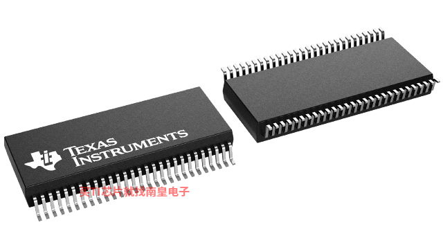
- 制造厂商:TI
- 产品类别:逻辑和电压转换
- 技术类目:缓冲器、驱动器和收发器 - 通用收发器
- 功能描述:具有三态输出的 3.3V ABT 16 位总线收发器和寄存器
- 点击这里打开及下载SN74LVT16646的技术文档资料
- TI代理渠道,提供当日发货、严格的质量标准,满足您的目标价格

The 'LVT16646 are 16-bit bus transceivers designed for low-voltage (3.3-V) VCC operation, but with the capability to provide a TTL interface to a 5-V system environment.
These devices can be used as two 8-bit transceivers or one 16-bit transceiver. Data on the A or B bus is clocked into the registers on the low-to-high transition of the appropriate clock (CLKAB or CLKBA) input. Figure 1 illustrates the four fundamental bus-management functions that can be performed with the ´LVT16646.
Output-enable (OE\) and direction-control (DIR) inputs are provided to control the transceiver functions. In the transceiver mode, data present at the high-impedance port may be stored in either register or in both. The select-control (SAB and SBA) inputs can multiplex stored and real-time (transparent mode) data. The circuitry used for select control eliminates the typical decoding glitch that occurs in a multiplexer during the transition between stored and real-time data. The direction control (DIR) determines which bus receives data when OE\ is low. In the isolation mode (OE\ high), A data may be stored in one register and/or B data may be stored in the other register.
When an output function is disabled, the input function is still enabled and may be used to store and transmit data. Only one of the two buses, A or B, may be driven at a time.
Active bus-hold circuitry holds unused or undriven inputs at a valid logic state. Use of pullup or pulldown resistors with the bus-hold circuitry is not recommended.
These devices are fully specified for hot-insertion applications using Ioff and power-up 3-state. The Ioff circuitry disables the outputs, preventing damaging current backflow through the devices when they are powered down. The power-up 3-state circuitry places the outputs in the high-impedance state during power up and power down, which prevents driver conflict.
To ensure the high-impedance state during power up or power down, OE\ should be tied to VCC through a pullup resistor; the minimum value of the resistor is determined by the current-sinking capability of the driver.
- Members of the Texas Instruments Widebus? Family
- State-of-the-Art Advanced BiCMOS Technology (ABT) Design for 3.3-V Operation and Low-Static Power Dissipation
- Support Mixed-Mode Signal Operation (5-V Input and Output Voltages With 3.3-V VCC)
- Support Unregulated Battery Operation Down to 2.7 V
- Typical VOLP (Output Ground Bounce) < 0.8 V at VCC = 3.3 V, TA = 25°C
- Bus-Hold Data Inputs Eliminate the Need for External Pullup Resistors
- Ioff and Power-Up 3-State Support Hot Insertion
- Distributed VCC and GND Pin Configuration Minimizes High-Speed Switching Noise
- Flowthrough Architecture Optimizes PCB Layout
- Latch-Up Performance Exceeds 500 mA Per JEDEC Standard JESD-17
- ESD Protection Exceeds JESD 22
- 2000-V Human-Body Model (A114-A)
- 200-V Machine Model (A115-A)
Widebus is a trademark of Texas Instruments.
- IOL (Max) (mA)
- 64
- IOH (Max) (mA)
- -32
- Technology Family
- LVT
- Rating
- Catalog
- Operating temperature range (C)
- -40 to 85
SN74LVT16646的完整型号有:SN74LVT16646DL,以下是这些产品的关键参数及官网采购报价:
SN74LVT16646DL,工作温度:-40 to 85,封装:SSOP (DL)-56,包装数量MPQ:20个,MSL 等级/回流焊峰值温度:Level-1-260C-UNLIM,引脚镀层/焊球材料:NIPDAU,TI官网SN74LVT16646DL的批量USD价格:7.211(1000+)

SN74LVT16646DL,工作温度:-40 to 85,封装:SSOP (DL)-56,包装数量MPQ:20个,MSL 等级/回流焊峰值温度:Level-1-260C-UNLIM,引脚镀层/焊球材料:NIPDAU,TI官网SN74LVT16646DL的批量USD价格:7.211(1000+)


