- 制造厂商:TI
- 产品类别:逻辑和电压转换
- 技术类目:触发器、锁存器和寄存器 - D 型锁存器
- 功能描述:具有三态输出的 3.3V ABT 八路透明 D 类锁存器
- 点击这里打开及下载SN74LVT573的技术文档资料
- TI代理渠道,提供当日发货、严格的质量标准,满足您的目标价格

These octal latches are designed specifically for low-voltage (3.3-V) VCC operation, but with the capability to provide a TTL interface to a 5-V system environment.
The eight latches of the 'LVT573 are transparent D-type latches. While the latch-enable (LE) input is high, the Q outputs follow the data (D) inputs. When LE is taken low, the Q outputs are latched at the logic levels set up at the D inputs.
A buffered output-enable ![]() input can be used to place the eight outputs in either a normal logic state (high or low logic levels) or a high-impedance state. In the high-impedance state, the outputs neither load nor drive the bus lines significantly. The high-impedance state and increased drive provide the capability to drive bus lines without need for interface or pullup components.
input can be used to place the eight outputs in either a normal logic state (high or low logic levels) or a high-impedance state. In the high-impedance state, the outputs neither load nor drive the bus lines significantly. The high-impedance state and increased drive provide the capability to drive bus lines without need for interface or pullup components. ![]() does not affect the internal operations of the latches. Old data can be retained or new data can be entered while the outputs are in the high-impedance state.
does not affect the internal operations of the latches. Old data can be retained or new data can be entered while the outputs are in the high-impedance state.
Active bus-hold circuitry is provided to hold unused or floating data inputs at a valid logic level.
To ensure the high-impedance state during power up or power down, ![]() should be tied to VCC through a pullup resistor; the minimum value of the resistor is determined by the current-sinking capability of the driver.
should be tied to VCC through a pullup resistor; the minimum value of the resistor is determined by the current-sinking capability of the driver.
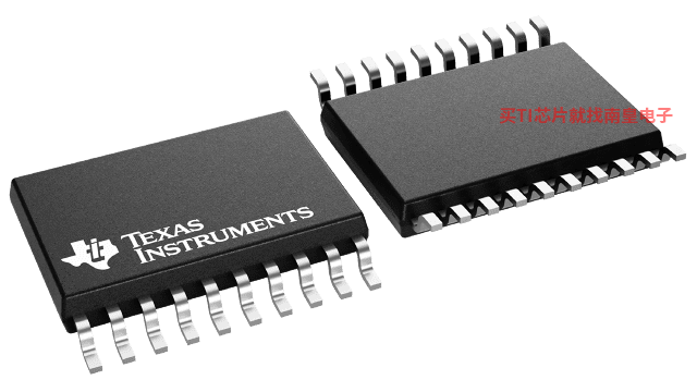
The SN74LVT573 is available in TI's shrink small-outline package (DB), which provides the same I/O pin count and functionality of standard small-outline packages in less than half the printed-circuit-board area.
The SN54LVT573 is characterized for operation over the full military temperature range of -55°C to 125°C. The SN74LVT573 is characterized for operation from -40°C to 85°C.
- State-of-the-Art Advanced BiCMOS Technology (ABT) Design for 3.3-V Operation and Low Static Power Dissipation
- Support Mixed-Mode Signal Operation (5-V Input and Output Voltages With 3.3-V VCC)
- Support Unregulated Battery Operation Down to 2.7 V
- Typical VOLP (Output Ground Bounce)< 0.8 V at VCC = 3.3 V, TA = 25°C
- ESD Protection Exceeds 2000 V Per MIL-STD-883C, Method 3015; Exceeds 200 V Using Machine Model (C = 200 pF, R = 0)
- Latch-Up Performance Exceeds 500 mA Per JEDEC Standard JESD-17
- Bus-Hold Data Inputs Eliminate the Need for External Pullup Resistors
- Support Live Insertion
- Package Options Include Plastic Small-Outline (DW), Shrink Small-Outline (DB), and Thin Shrink Small-Outline (PW) Packages, Ceramic Chip Carriers (FK), Ceramic Flat (W) Packages, and Ceramic (J) DIPs
- Number of channels (#)
- 8
- Technology Family
- LVT
- Supply voltage (Min) (V)
- 2.7
- Supply voltage (Max) (V)
- 3.6
- Input type
- TTL-Compatible CMOS
- Output type
- 3-State
- Clock Frequency (Max) (MHz)
- 160
- IOL (Max) (mA)
- 16
- IOH (Max) (mA)
- -16
- ICC (Max) (uA)
- 5000
- Features
- High speed (tpd 10-50ns)
SN74LVT573的完整型号有:SN74LVT573DW、SN74LVT573PWR,以下是这些产品的关键参数及官网采购报价:
SN74LVT573DW,工作温度:-40 to 85,封装:SOIC (DW)-20,包装数量MPQ:25个,MSL 等级/回流焊峰值温度:Level-1-260C-UNLIM,引脚镀层/焊球材料:NIPDAU,TI官网SN74LVT573DW的批量USD价格:2.722(1000+)
SN74LVT573PWR,工作温度:-40 to 85,封装:TSSOP (PW)-20,包装数量MPQ:2000个,MSL 等级/回流焊峰值温度:Level-1-260C-UNLIM,引脚镀层/焊球材料:NIPDAU,TI官网SN74LVT573PWR的批量USD价格:.869(1000+)

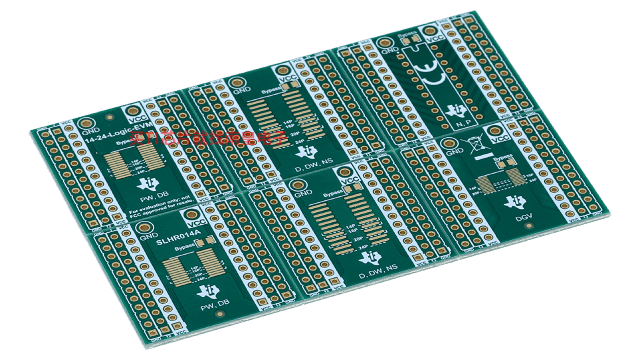
14-24-LOGIC-EVM ― 支持 14 到 24 引脚 PW、DB、D、DW、NS、DYY 和 DGV 封装的通用逻辑 EVM
该 EVM 设计用于支持采用 14 至 24 引脚 D、DW、DB、NS、PW、DYY 或 DGV 封装的任何逻辑器件。