- ���쳧�̣�TI
- ��Ʒ����ӿ�
- ������Ŀ�������ӿ�
- ������������ǿ�Ͳ�ƷǶ��ʽ�������߿����� Ieee Std 1149.1 (Jtag) Tap ��������
- ������������SN74LVT8980A-EP�ļ����ĵ�����
- TI�����������ṩ���շ������ϸ������������������Ŀ��۸�

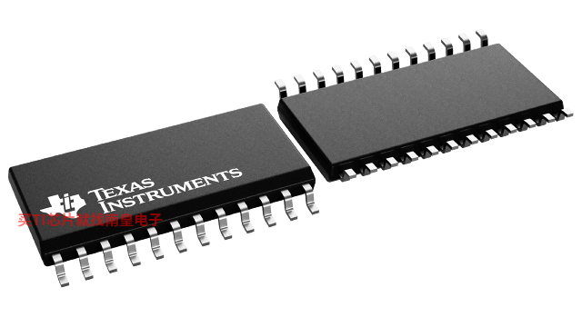
The SN74LVT8980A embedded test-bus controllers (eTBCs) are members of the TI broad family of testability integrated circuits. This family of devices supports IEEE Std 1149.1-1990 boundary scan to facilitate testing of complex circuit assemblies. Unlike most other devices of this family, the eTBCs are not boundary-scannable devices; rather, their function is to master an IEEE Std 1149.1 (JTAG) test access port (TAP) under the command of an embedded host microprocessor/microcontroller. Thus, the eTBCs enable the practical and effective use of the IEEE Std 1149.1 test-access infrastructure to support embedded/built-in test, emulation, and configuration/maintenance facilities at board and system levels.
The eTBCs master all TAP signals required to support one 4- or 5-wire IEEE Std 1149.1 serial test bus: test clock (TCK), test mode select (TMS), test data input (TDI), test data output (TDO), and test reset (TRST)\. All such signals can be connected directly to the associated target IEEE Std 1149.1 devices without need for additional logic or buffering. However, as well as being directly connected, the TMS, TDI, and TDO signals can be connected to distant target IEEE Std 1149.1 devices via a pipeline, with a retiming delay of up to 15 TCK cycles; the eTBCs automatically handle all associated serial-data justification.
Conceptually, the eTBCs operate as simple 8-bit memory- or I/O-mapped peripherals to a microprocessor/microcontroller (host). High-level commands and parallel data are passed to/from the eTBCs via their generic host interface, which includes an 8-bit data bus (D7-D0) and a 3-bit address bus (A2-A0). Read/write select (R/W\) and strobe (STRB)\ signals are implemented so that the critical host-interface timing is independent of the CLKIN period. An asynchronous ready (RDY) indicator is provided to hold off, or insert wait states into, a host read/write cycle when the eTBCs cannot respond immediately to the requested read/write operation.
High-level commands are issued by the host to cause the eTBCs to generate the TMS sequences necessary to move the test bus from any stable TAP-controller state to any other such stable state, to scan instruction or data through test registers in target devices, and/or to execute instructions in the Run-Test/Idle TAP state. A 32-bit counter can be programmed to allow a predetermined number of scan or execute cycles.
During scan operations, serial data that appears at the TDI input is transferred into a serial to 4 × 8-bit-parallel first-in/first-out (FIFO) read buffer, which can then be read by the host to obtain the return serial-data stream up to eight bits at a time. Serial data that is to be transmitted from the TDO output is written by the host, up to eight bits at a time, to a 4 × 8-bit-parallel to serial FIFO write buffer.
In addition to such simple state-movement, scan, and run-test operations, the eTBCs support several additional commands that provide for input-only scans, output-only scans, recirculate scans (in which TDI is mirrored back to TDO), and a scan mode that generates the protocols used to support multidrop TAP configurations using TI’s addressable scan port. Two loopback modes also are supported that allow the microprocessor/microcontroller host to monitor the TDO or TMS data streams output by the eTBCs.
The eTBCs’ flexible clocking architecture allows the user to choose between free-running (in which the TCK always follows CLKIN) and gated modes (in which the TCK output is held static except during state-move, run-test, or scan cycles) as well as to divide down TCK from CLKIN. A discrete mode also is available in which the TAP is driven strictly by read/write cycles under full control of the microprocessor/microcontroller host. These features ensure that virtually any IEEE Std 1149.1 target device or device chain can be serviced by the eTBCs, even where such may not fully comply to IEEE Std 1149.1.
While most operations of the eTBCs are synchronous to CLKIN, a test-output enable (TOE)\ is provided for output control of the TAP outputs, and a reset (RST)\ input is provided for hardware reset of the eTBCs. The former can be used to disable the eTBCs so that an external controller can master the associated IEEE Std 1149.1 test bus.
- Controlled Baseline
- One Assembly/Test Site, One Fabrication Site
- Enhanced Diminishing Manufacturing Sources (DMS) Support
- Enhanced Product-Change Notification
- Qualification Pedigree
- Members of Texas Instruments Broad Family of Testability Products Supporting IEEE Std 1149.1-1990 (JTAG) Test Access Port (TAP) and Boundary-Scan Architecture
- Provide Built-In Access to IEEE Std 1149.1 Scan-Accessible Test/Maintenance Facilities at Board and System Levels
- While Powered at 3.3 V, the TAP Interface Is Fully 5-V Tolerant for Mastering Both 5-V and/or 3.3-V IEEE Std 1149.1 Targets
- Simple Interface to Low-Cost 3.3-V Microprocessors/Microcontrollers Via 8-Bit Asynchronous Read/Write Data Bus
- Easy Programming Via Scan-Level Command Set and Smart TAP Control
- Transparently Generate Protocols to Support Multidrop TAP Configurations Using TI��s Addressable Scan Port
- Flexible TCK Generator Provides Programmable Division, Gated-TCK, and Free-Running-TCK Modes
- Discrete TAP Control Mode Supports Arbitrary TMS/TDI Sequences for Noncompliant Targets
- Programmable 32-Bit Test Cycle Counter Allows Virtually Unlimited Scan/Test Length
- Accommodate Target Retiming (Pipeline) Delays of up to 15 TCK Cycles
- Test Output Enable (TOE)\ Allows for External Control of TAP Signals
- High-Drive Outputs (�C32-mA IOH, 64-mA IOL) at TAP Support Backplane Interface and/or High Fanout
Component qualification in accordance with JEDEC and industry standards to ensure reliable operation over an extended temperature range. This includes, but is not limited to, Highly Accelerated Stress Test (HAST) or biased 85/85, temperature cycle, autoclave or unbiased HAST, electromigration, bond intermetallic life, and mold compound life. Such qualification testing should not be viewed as justifying use of this component beyond specified performance and environmental limits.
- Operating temperature range (C)
- -40 to 85
SN74LVT8980A-EP�������ͺ��У�SN74LVT8980AIDWREP��V62/03668-01XE����������Щ��Ʒ�Ĺؼ������������ɹ����ۣ�
SN74LVT8980AIDWREP�������¶ȣ�-40 to 85����װ��SOIC (DW)-24����װ����MPQ��2000����MSL �ȼ�/��������ֵ�¶ȣ�Level-1-260C-UNLIM�����ŶƲ�/������ϣ�NIPDAU��TI����SN74LVT8980AIDWREP������USD�۸�11.723��1000+��
V62/03668-01XE�������¶ȣ�-40 to 85����װ��SOIC (DW)-24����װ����MPQ��2000����MSL �ȼ�/��������ֵ�¶ȣ�Level-1-260C-UNLIM�����ŶƲ�/������ϣ�NIPDAU��TI����V62/03668-01XE������USD�۸�11.723��1000+��

PSPICE-FOR-TI �� ������ TI ��ƺ�ģ��ߵ� PSpice
PSpice for TI ���ṩ��������ģ���·���ܵ���ƺͷ��滷�����˹�����ȫ����ƺͷ�����ʹ�� Cadence ��ģ��������档PSpice for TI �����ʹ�ã�����ҵ�ڳ����ģ�Ϳ�֮һ���������ǵ�ģ��͵�Դ��Ʒϵ���Լ���ѡ��ģ����Ϊģ�͡�����?PSpice for TI ����ƺͷ��滷���������õ�ģ�Ϳ⣬���ɶԸ��ӵĻ���ź���ƽ��з��档�����������ն��豸��ƺ�ԭ�ͽ��������Ȼ���ٽ��в��ֺ����죬�����̲�Ʒ����ʱ�䲢���Ϳ����ɱ���
��?PSpice for TI ��ƺͷ��湤���У����������� TI (...)
TINA-TI �� ���� SPICE ��ģ��������
TINA-TI �ṩ�� SPICE ���еĴ�ͳֱ����˲̬��Ƶ������Լ����ࡣTINA ���й㷺�ĺ������ܣ�����������ϣ���ķ�ʽ���ý���ĸ�ʽ����������������ѡ�����벨�Ρ�̽���·�ڵ��ѹ�Ͳ��Ρ�TINA ��ԭ��ͼ����dz�ֱ�� - �����ġ��������š���TINA-TI ��װ��Ҫ��Լ 500MB��ֱ�Ӱ�װ�������ж��Ҳ�����ס������������϶��ᰮ�����֡�
TINA �ǵ������� (TI) ר�е� DesignSoft ��Ʒ������Ѱ汾���������Ĺ��ܣ�����֧�������� TINA ���ṩ��ijЩ�������ܡ�
�����ȡ���� TINA-TI ģ�͵������б�������ģ�SpiceRack - �����б�
��Ҫ HSpice (...)


