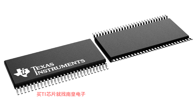
- 制造厂商:TI
- 产品类别:逻辑和电压转换
- 技术类目:缓冲器、驱动器和收发器 - 通用收发器
- 功能描述:具有三态输出的增强型产品 3.3V Abt 16 位总线收发器和寄存器
- 点击这里打开及下载SN74LVTH16652-EP的技术文档资料
- TI代理渠道,提供当日发货、严格的质量标准,满足您的目标价格

The SN74LVTH16652 is a 16-bit bus transceiver designed for low-voltage (3.3-V) VCC operation, but with the capability to provide a TTL interface to a 5-V system environment. These devices can be used as two 8-bit transceivers or one 16-bit transceiver.
Output-enable (OEAB and OEBA\) inputs are provided to control the transceiver functions. Select-control (SAB and SBA) inputs are provided to select whether real-time or stored data is transferred. A low input level selects real-time data, and a high input level selects stored data. The circuitry used for select control eliminates the typical decoding glitch that occurs in a multiplexer during the transition between stored and real-time data. Figure 1 illustrates the four fundamental bus-management functions that can be performed with the SN74LVTH16652.
Data on the A or B bus, or both, can be stored in the internal D flip-flops by low-to-high transitions at the appropriate clock (CLKAB or CLKBA) inputs, regardless of the levels on the select-control or output-enable inputs. When SAB and SBA are in the real-time transfer mode, it also is possible to store data without using the internal D-type flip-flops by simultaneously enabling OEAB and OEBA\. In this configuration, each output reinforces its input. When all other data sources to the two sets of bus lines are at high impedance, each set of bus lines remains at its last level configuration.
When VCC is between 0 and 1.5 V, the device is in the high-impedance state during power up or power down. However, to ensure the high-impedance state above 1.5 V, OE\ should be tied to VCC through a pullup resistor, and OE should be tied to GND through a pulldown resistor; the minimum value of the resistor is determined by the current-sinking/current-sourcing capability of the driver.
Active bus-hold circuitry is provided to hold unused or floating data inputs at a valid logic level.
This device is fully specified for hot-insertion applications using Ioff and power-up 3-state. The Ioff circuitry disables the outputs, preventing damaging current backflow through the device when it is powered down. The power-up 3-state circuitry places the outputs in the high-impedance state during power up and power down, which prevents driver conflict.
- Controlled Baseline
- One Assembly/Test Site, One Fabrication Site
- Enhanced Diminishing Manufacturing Sources (DMS) Support
- Enhanced Product-Change Notification
- Qualification Pedigree
- Member of the Texas Instruments Widebus? Family
- State-of-the-Art Advanced BiCMOS Technology (ABT) Design for 3.3-V Operation and Low Static-Power Dissipation
- Supports Mixed-Mode Signal Operation (5-V Input and Output Voltages With 3.3-V VCC)
- Supports Unregulated Battery Operation Down To 2.7 V
- Typical VOLP (Output Ground Bounce) <0.8 V at VCC = 3.3 V, TA = 25°C
- Ioff and Power-Up 3-State Support Hot Insertion
- Bus Hold on Data Inputs Eliminates the Need for External Pullup/Pulldown Resistors
- Distributed VCC and GND Pins Minimize High-Speed Switching Noise
- Flow-Through Architecture Optimizes PCB Layout
- Latch-Up Performance Exceeds 500 mA Per JESD 17
- ESD Protection Exceeds 2000 V Per MIL-STD-883, Method 3015; Exceeds 200 V Using Machine Model (C = 200 pF, R = 0)
- Thin Shrink Small-Outline (DGG) Package
Component qualification in accordance with JEDEC and industry standards to ensure reliable operation over an extended temperature range. This includes, but is not limited to, Highly Accelerated Stress Test (HAST) or biased 85/85, temperature cycle, autoclave or unbiased HAST, electromigration, bond intermetallic life, and mold compound life. Such qualification testing should not be viewed as justifying use of this component beyond specified performance and environmental limits. Widebus is a trademark of Texas Instruments.
- IOL (Max) (mA)
- 64
- IOH (Max) (mA)
- -64
- Technology Family
- LVT
- Rating
- HiRel Enhanced Product
- Operating temperature range (C)
- -40 to 85
SN74LVTH16652-EP的完整型号有:CLVTH16652IDGGREP、V62/04717-01XE,以下是这些产品的关键参数及官网采购报价:
CLVTH16652IDGGREP,工作温度:-40 to 85,封装:TSSOP (DGG)-56,包装数量MPQ:2000个,MSL 等级/回流焊峰值温度:Level-1-260C-UNLIM,引脚镀层/焊球材料:NIPDAU,TI官网CLVTH16652IDGGREP的批量USD价格:3.223(1000+)
V62/04717-01XE,工作温度:-40 to 85,封装:TSSOP (DGG)-56,包装数量MPQ:2000个,MSL 等级/回流焊峰值温度:Level-1-260C-UNLIM,引脚镀层/焊球材料:NIPDAU,TI官网V62/04717-01XE的批量USD价格:3.223(1000+)


