- 制造厂商:TI
- 产品类别:逻辑和电压转换
- 技术类目:缓冲器、驱动器和收发器 - 通用收发器
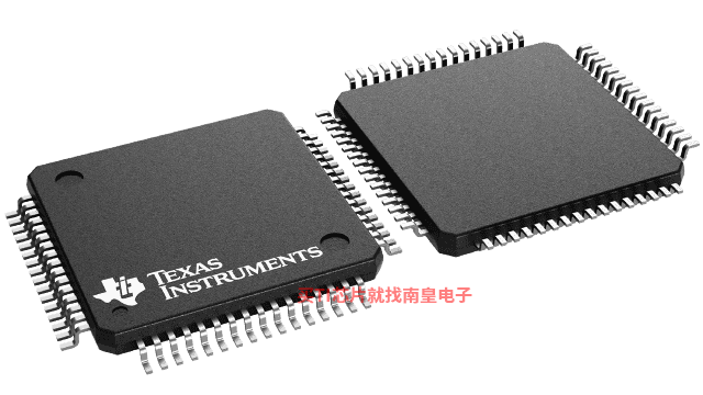
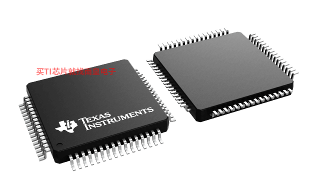
- 功能描述:具有 20 位通用总线收发器的 3.3V ABT 扫描测试设备
- 点击这里打开及下载SN74LVTH18504A的技术文档资料
- TI代理渠道,提供当日发货、严格的质量标准,满足您的目标价格

The 'LVTH18504A and 'LVTH182504A scan test devices with 20-bit universal bus transceivers are members of the Texas Instruments (TI) SCOPE testability integrated-circuit family. This family of devices supports IEEE Std 1149.1-1990 boundary scan to facilitate testing of complex circuit-board assemblies. Scan access to the test circuitry is accomplished via the 4-wire test access port (TAP) interface.
Additionally, these devices are designed specifically for low-voltage (3.3-V) VCC operation, but with the capability to provide a TTL interface to a 5-V system environment.
In the normal mode, these devices are 20-bit universal bus transceivers that combine D-type latches and D-type flip-flops to allow data flow in transparent, latched, or clocked modes. The test circuitry can be activated by the TAP to take snapshot samples of the data appearing at the device pins or to perform a self-test on the boundary-test cells. Activating the TAP in the normal mode does not affect the functional operation of the SCOPE universal bus transceivers.
Data flow in each direction is controlled by output-enable (![]() and
and ![]() ), latch-enable (LEAB and LEBA), clock-enable (
), latch-enable (LEAB and LEBA), clock-enable (![]() and
and ![]() ), and clock (CLKAB and CLKBA) inputs. For A-to-B data flow, the device operates in the transparent mode when LEAB is high. When LEAB is low, the A-bus data is latched while
), and clock (CLKAB and CLKBA) inputs. For A-to-B data flow, the device operates in the transparent mode when LEAB is high. When LEAB is low, the A-bus data is latched while ![]() is high and/or CLKAB is held at a static low or high logic level. Otherwise, if LEAB is low and
is high and/or CLKAB is held at a static low or high logic level. Otherwise, if LEAB is low and ![]() is low, A-bus data is stored on a low-to-high transition of CLKAB. When
is low, A-bus data is stored on a low-to-high transition of CLKAB. When ![]() is low, the B outputs are active. When
is low, the B outputs are active. When ![]() is high, the B outputs are in the high-impedance state. B-to-A data flow is similar to A-to-B data flow, but uses the
is high, the B outputs are in the high-impedance state. B-to-A data flow is similar to A-to-B data flow, but uses the ![]() , LEBA,
, LEBA,![]() , and CLKBA inputs.
, and CLKBA inputs.
In the test mode, the normal operation of the SCOPE universal bus transceivers is inhibited, and the test circuitry is enabled to observe and control the I/O boundary of the device. When enabled, the test circuitry performs boundary-scan test operations according to the protocol described in IEEE Std 1149.1-1990.
Four dedicated test pins are used to observe and control the operation of the test circuitry: test data input (TDI), test data output (TDO), test mode select (TMS), and test clock (TCK). Additionally, the test circuitry performs other testing functions, such as parallel-signature analysis (PSA) on data inputs and pseudo-random pattern generation (PRPG) from data outputs. All testing and scan operations are synchronized to the TAP interface.
Active bus-hold circuitry is provided to hold unused or floating data inputs at a valid logic level.
The B-port outputs of 'LVTH182504A, which are designed to source or sink up to 12 mA, include equivalent 25-![]() series resistors to reduce overshoot and undershoot.
series resistors to reduce overshoot and undershoot.
The SN54LVTH18504A and SN54LVTH182504A are characterized for operation over the full military temperature range of -55°C to 125°C. The SN74LVTH18504A and SN74LVTH182504A are characterized for operation from -40°C to 85°C.
- Members of the Texas Instruments SCOPETM Family of Testability Products
- Members of the Texas Instruments WidebusTM Family
- State-of-the-Art 3.3-V ABT Design Supports Mixed-Mode Signal Operation (5-V Input and Output Voltages With 3.3-V VCC)
- Support Unregulated Battery Operation Down to 2.7 V
- UBTTM (Universal Bus Transceiver) Combines D-Type Latches and D-Type Flip-Flops for Operation in Transparent, Latched, or Clocked Mode
- Bus Hold on Data Inputs Eliminates the Need for External Pullup/Pulldown Resistors
- B-Port Outputs of 'LVTH182504A Devices Have Equivalent 25- Series Resistors, So No External Resistors Are Required
- Compatible With the IEEE Std 1149.1-1990 (JTAG) Test Access Port and Boundary-Scan Architecture
- SCOPE Instruction Set
- IEEE Std 1149.1-1990 Required Instructions and Optional CLAMP and HIGHZ
- Parallel-Signature Analysis at Inputs
- Pseudo-Random Pattern Generation From Outputs
- Sample Inputs/Toggle Outputs
- Binary Count From Outputs
- Device Identification
- Even-Parity Opcodes
- Packaged in 64-Pin Plastic Thin Quad Flat (PM) Packages Using 0.5-mm Center-to-Center Spacings and 68-Pin Ceramic Quad Flat (HV) Packages Using 25-mil Center-to-Center Spacings
SCOPE, UBT, and Widebus are trademarks of Texas Instruments Incorporated.
- IOL (Max) (mA)
- 32
- IOH (Max) (mA)
- -32
- Technology Family
- LVT
- Rating
- Catalog
- Operating temperature range (C)
- -40 to 85
SN74LVTH18504A的完整型号有:SN74LVTH18504APM、SN74LVTH18504APMR,以下是这些产品的关键参数及官网采购报价:
SN74LVTH18504APM,工作温度:-40 to 85,封装:LQFP (PM)-64,包装数量MPQ:160个,MSL 等级/回流焊峰值温度:Level-3-260C-168 HR,引脚镀层/焊球材料:NIPDAU,TI官网SN74LVTH18504APM的批量USD价格:4.535(1000+)
SN74LVTH18504APMR,工作温度:-40 to 85,封装:LQFP (PM)-64,包装数量MPQ:1000个,MSL 等级/回流焊峰值温度:Level-3-260C-168 HR,引脚镀层/焊球材料:NIPDAU,TI官网SN74LVTH18504APMR的批量USD价格:3.779(1000+)