- 制造厂商:TI
- 产品类别:逻辑和电压转换
- 技术类目:缓冲器、驱动器和收发器 - 同相缓冲器和驱动器
- 功能描述:具有总线保持、TTL 兼容型 CMOS 输入和三态输出的 8 通道、2.7V 至 3.6V 缓冲器
- 点击这里打开及下载SN74LVTH541的技术文档资料
- TI代理渠道,提供当日发货、严格的质量标准,满足您的目标价格

These octal buffers/drivers are designed specifically for low-voltage (3.3-V) VCC operation, but with the capability to provide a TTL interface to a 5-V system environment.
The ’LVTH541 devices are ideal for driving bus lines or buffer memory address registers. These devices feature inputs and outputs on opposite sides of the package that facilitate printed circuit board layout.
The 3-state control gate is a 2-input AND gate with active-low inputs so that if either output-enable (OE1\ or OE2\) input is high, all outputs are in the high-impedance state.
Active bus-hold circuitry holds unused or undriven inputs at a valid logic state. Use of pullup or pulldown resistors with the bus-hold circuitry is not recommended.
When VCC is between 0 and 1.5 V, the devices are in the high-impedance state during power up or power down. However, to ensure the high-impedance state above 1.5 V, OE\ should be tied to VCC through a pullup resistor; the minimum value of the resistor is determined by the current-sinking capability of the driver.
These devices are fully specified for hot-insertion applications using Ioff and power-up 3-state. The Ioff circuitry disables the outputs, preventing damaging current backflow through the devices when they are powered down. The power-up 3-state circuitry places the outputs in the high-impedance state during power up and power down, which prevents driver conflict.
- Support Mixed-Mode Signal Operation (5-V Input and Output Voltages With 3.3-V VCC)
- Typical VOLP (Output Ground Bounce) <0.8 V at VCC = 3.3 V, TA = 25°C
- Support Unregulated Battery Operation Down to 2.7 V
- Ioff and Power-Up 3-State Support Hot Insertion
- Bus Hold on Data Inputs Eliminates the Need for External Pullup/Pulldown Resistors
- Latch-Up Performance Exceeds 500 mA Per JESD 17
- ESD Protection Exceeds JESD 22
- 2000-V Human-Body Model (A114-A)
- 200-V Machine Model (A115-A)
- Technology Family
- LVT
- Supply voltage (Min) (V)
- 2.7
- Supply voltage (Max) (V)
- 3.6
- Number of channels (#)
- 8
- IOL (Max) (mA)
- 64
- ICC (Max) (uA)
- 5000
- IOH (Max) (mA)
- -32
- Input type
- TTL-Compatible CMOS
- Output type
- 3-State
- Features
- Ultra high speed (tpd <5ns), Partial power down (Ioff), Over-voltage tolerant inputs, Power up 3-state, Bus-hold
- Rating
- Catalog
SN74LVTH541的完整型号有:SN74LVTH541DBR、SN74LVTH541DW、SN74LVTH541DWR、SN74LVTH541NSR、SN74LVTH541PW、SN74LVTH541PWR,以下是这些产品的关键参数及官网采购报价:
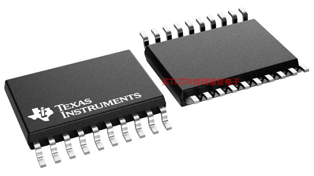
SN74LVTH541DBR,工作温度:-40 to 85,封装:SSOP (DB)-20,包装数量MPQ:2000个,MSL 等级/回流焊峰值温度:Level-1-260C-UNLIM,引脚镀层/焊球材料:NIPDAU,TI官网SN74LVTH541DBR的批量USD价格:.724(1000+)
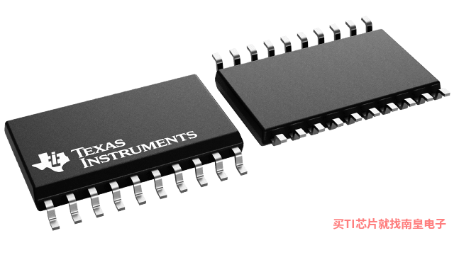
SN74LVTH541DW,工作温度:-40 to 85,封装:SOIC (DW)-20,包装数量MPQ:25个,MSL 等级/回流焊峰值温度:Level-1-260C-UNLIM,引脚镀层/焊球材料:NIPDAU,TI官网SN74LVTH541DW的批量USD价格:.79(1000+)
SN74LVTH541DWR,工作温度:-40 to 85,封装:SOIC (DW)-20,包装数量MPQ:2000个,MSL 等级/回流焊峰值温度:Level-1-260C-UNLIM,引脚镀层/焊球材料:NIPDAU,TI官网SN74LVTH541DWR的批量USD价格:.658(1000+)
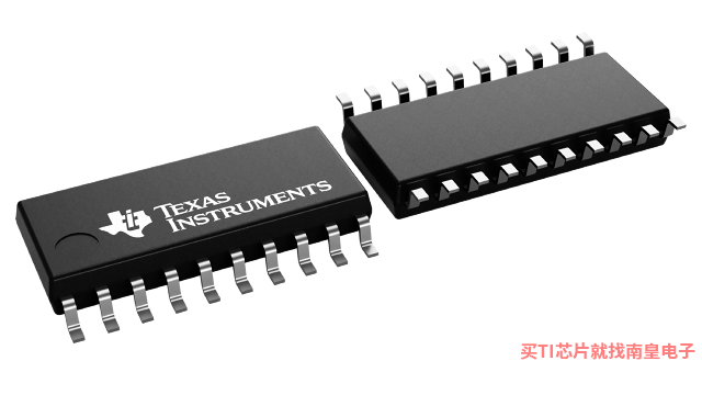
SN74LVTH541NSR,工作温度:-40 to 85,封装:SO (NS)-20,包装数量MPQ:2000个,MSL 等级/回流焊峰值温度:Level-1-260C-UNLIM,引脚镀层/焊球材料:NIPDAU,TI官网SN74LVTH541NSR的批量USD价格:.724(1000+)
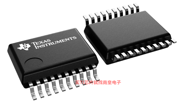
SN74LVTH541PW,工作温度:-40 to 85,封装:TSSOP (PW)-20,包装数量MPQ:70个,MSL 等级/回流焊峰值温度:Level-1-260C-UNLIM,引脚镀层/焊球材料:NIPDAU,TI官网SN74LVTH541PW的批量USD价格:.79(1000+)
SN74LVTH541PWR,工作温度:-40 to 85,封装:TSSOP (PW)-20,包装数量MPQ:2000个,MSL 等级/回流焊峰值温度:Level-1-260C-UNLIM,引脚镀层/焊球材料:NIPDAU,TI官网SN74LVTH541PWR的批量USD价格:.618(1000+)

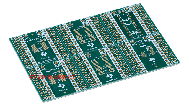
14-24-LOGIC-EVM ― 支持 14 到 24 引脚 PW、DB、D、DW、NS、DYY 和 DGV 封装的通用逻辑 EVM
该 EVM 设计用于支持采用 14 至 24 引脚 D、DW、DB、NS、PW、DYY 或 DGV 封装的任何逻辑器件。