- 制造厂商:TI
- 产品类别:逻辑和电压转换
- 技术类目:专用逻辑 IC - 数字多路信号分离器和解码器
- 功能描述:双路 2 线路至 4 线路解码器/多路解复用器
- 点击这里打开及下载SN74S139A的技术文档资料
- TI代理渠道,提供当日发货、严格的质量标准,满足您的目标价格

These Schottky-clamped TTL MSI circuits are designed to be used in high-performance memory-decoding or data-routing applications requiring very short propagation delay times. In high-performance memory systems, these decoders can be used to minimize the effects of system decoding. When employed with high-speed memories utilizing a fast-enable circuit, the delay times of these decoders and the enable time of the memory are usually less than the typical access time of the memory. This means that the effective system delay introduced by the Schottky-clamped system decoder is negligible.
The circuit comprises two individual two-line to four-line decoders in a single package. The active-low enable input can be used as a data line in demultiplexing applications.
All of these decoders/demultiplexers feature fully buffered inputs, each of which represents only one normalized load to its driving circuit. All inputs are clamped with high-performance Schottky diodes to suppress line-ringing and to simplify system design. The SN54LS139A and SN54S139 are characterized for operation range of –55°C to 125°C. The SN74LS139A and SN74S139A are characterized for operation from 0°C to 70°C.
- Designed Specifically for High-Speed:
- Memory Decoders
- Data Transmission Systems
- Two Fully Independent 2- to 4-Line Decoders/Demultiplexers
- Schottky clamped for High Performance
- Technology Family
- S
- Number of channels (#)
- 2
- Operating temperature range (C)
- 0 to 70
- Rating
- Catalog
- ICC (Max) (uA)
- 90000
SN74S139A的完整型号有:SN74S139AD、SN74S139AN,以下是这些产品的关键参数及官网采购报价:
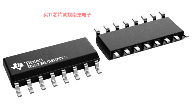
SN74S139AD,工作温度:0 to 70,封装:SOIC (D)-16,包装数量MPQ:40个,MSL 等级/回流焊峰值温度:Level-1-260C-UNLIM,引脚镀层/焊球材料:NIPDAU,TI官网SN74S139AD的批量USD价格:.924(1000+)
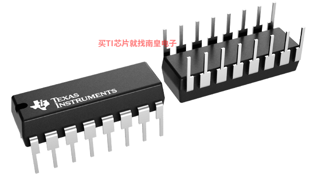
SN74S139AN,工作温度:0 to 70,封装:PDIP (N)-16,包装数量MPQ:25个,MSL 等级/回流焊峰值温度:N/A for Pkg Type,引脚镀层/焊球材料:NIPDAU,TI官网SN74S139AN的批量USD价格:1.063(1000+)

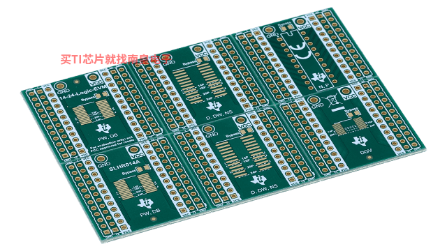
14-24-LOGIC-EVM ― 支持 14 到 24 引脚 PW、DB、D、DW、NS、DYY 和 DGV 封装的通用逻辑 EVM
该 EVM 设计用于支持采用 14 至 24 引脚 D、DW、DB、NS、PW、DYY 或 DGV 封装的任何逻辑器件。


