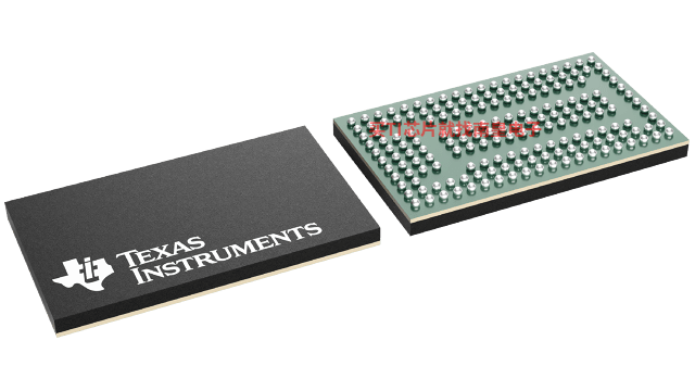
- 制造厂商:TI
- 产品类别:时钟和计时
- 技术类目:时钟缓冲器
- 功能描述:符合 JEDEC SSTE32882 标准且具有地址奇偶校验的 28 位至 56 位寄存缓冲器
- 点击这里打开及下载SN74SSQEC32882的技术文档资料
- TI代理渠道,提供当日发货、严格的质量标准,满足您的目标价格

This 1:2 or 26-bit 1:2 and 4-bit 1:1 registering clock driver with parity is designed for operation on DDR3 registered DIMMs with VDD of 1.5 V, on DDR3L registered DIMMs with VDD of 1.35 V and on DDR3U registered DIMMs with VDD of 1.25 V.
All inputs are 1.5 V, 1.35V and 1.25 V CMOS compatible. All outputs are CMOS drivers optimized to drive DRAM signals on terminated traces in DDR3 RDIMM applications. The clock outputs Yn and Yn and control net outputs DxCKEn, DxCSn and DxODTn can be driven with a different strength and skew to optimize signal integrity, compensate for different loading and equalize signal travel speed.
The SN74SSQEC32882 has two basic modes of operation associated with the Quad Chip Select Enable (QCSEN) input. When the QCSEN input pin is open (or pulled high), the component has two chip select inputs, DCS0 and DCS1, and two copies of each chip select output, QACS0, QACS1, QBCS0 and QBCS1. This is the "QuadCS disabled" mode. When the QCSEN input pin is pulled low, the component has four chip select inputs DCS[3:0], and four chip select outputs, QCS[3:0]. This is the "QuadCS enabled" mode. Through the remainder of this specification, DCS[n:0] will indicate all of the chip select inputs, where n=1 for QuadCS disabled, and n=3 for QuadCS enabled. QxCS[n:0] will indicate all of the chip select outputs.
The device also supports a mode where a single device can be mounted on the back side of a DIMM. If MIRROR=HIGH, Input Bus Termination (IBT) has to stay enabled for all input signals in this case.
The SN74SSQEC32882 operates from a differential clock (CK and CK). Data are registered at the crossing of CK going HIGH, and CK going LOW. This data could be either re-driven to the outputs or it could be used to access device internal control registers.
The input bus data integrity is protected by a parity function. All address and command input signals are added up and the last bit of the sum is compared to the parity signal delivered by the system at the input PAR_IN one clock cycle later. If they do not match the device pulls the open drain output ERROUT LOW. The control signals (DCKE0, DCKE1, DODT0, DODT1, DCS[n:0]) are not part of this computation.
The SN74SSQEC32882 implements different power saving mechanisms to reduce thermal power dissipation and to support system power down states. By disabling unused outputs the power consumption is further reduced.
The package is optimized to support high density DIMMs. By aligning input and output positions towards DIMM finger signal ordering and SDRAM ballout the device de-scrambles the DIMM traces allowing low cross talk design with low interconnect latency.
Edge controlled outputs reduce ringing and improve signal eye opening at the SDRAM inputs.
- JEDEC SSTE32882
- 1-to-2 Register Outputs and 1-to-4 Clock Pair Outputs Support Stacked DDR3 RDIMMs
- CKE Powerdown Mode for Optimized System Power Consumption
- 1.5V/1.35V/1.25V Phase Lock Loop Clock Driver for Buffering One Differential Clock Pair (CK and CK) and Distributing to Four Differential Outputs
- 1.5V/1.35V/1.25V CMOS Inputs
- Checks Parity on Command and Address (CS-Gated) Data Inputs
- Configurable Driver Strength
- Uses Internal Feedback Loop
- Optimized Power Consumption
- Function
- Memory interface
- Additive RMS jitter (Typ) (fs)
- 30
- Output frequency (Max) (MHz)
- 945
- Number of outputs
- 60
- Output supply voltage (V)
- 1.35
- Core supply voltage (V)
- 1.35
- Features
- DDR3 register
- Operating temperature range (C)
- 0 to 85
- Rating
- Catalog
- Output type
- CMOS
- Input type
- CMOS
SN74SSQEC32882的完整型号有:SN74SSQEC32882ZALR,以下是这些产品的关键参数及官网采购报价:
SN74SSQEC32882ZALR,工作温度:0 to 85,封装:NFBGA (ZAL)-176,包装数量MPQ:2000个,MSL 等级/回流焊峰值温度:Level-3-250C-168 HR,引脚镀层/焊球材料:SNAGCU,TI官网SN74SSQEC32882ZALR的批量USD价格:3.432(1000+)

PSPICE-FOR-TI ― 适用于 TI 设计和模拟工具的 PSpice
PSpice for TI 可提供帮助评估模拟电路功能的设计和仿真环境。此功能齐全的设计和仿真套件使用 Cadence 的模拟分析引擎。PSpice for TI 可免费使用,包括业内超大的模型库之一,涵盖我们的模拟和电源产品系列以及精选的模拟行为模型。借助?PSpice for TI 的设计和仿真环境及其内置的模型库,您可对复杂的混合信号设计进行仿真。创建完整的终端设备设计和原型解决方案,然后再进行布局和制造,可缩短产品上市时间并降低开发成本。
在?PSpice for TI 设计和仿真工具中,您可以搜索 TI (...)


