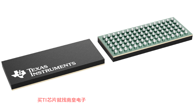
- 制造厂商:TI
- 产品类别:时钟和计时
- 技术类目:时钟缓冲器
- 功能描述:具有 SSTL_18 输入和输出的 500MHz、25 位可配置寄存缓冲器
- 点击这里打开及下载SN74SSTU32864的技术文档资料
- TI代理渠道,提供当日发货、严格的质量标准,满足您的目标价格

This 25-bit 1:1 or 14-bit 1:2 configurable registered buffer is designed for 1.7-V to 1.9-V VCC operation. In the 1:1 pinout configuration, only one device per DIMM is required to drive nine SDRAM loads. In the 1:2 pinout configuration, two devices per DIMM are required to drive 18 SDRAM loads.
All inputs are SSTL_18, except the LVCMOS reset (RESET)\ and LVCMOS control (Cn) inputs. All outputs are edge-controlled circuits optimized for unterminated DIMM loads and meet SSTL_18 specifications.
The SN74SSTU32864 operates from a differential clock (CLK and CLK\). Data are registered at the crossing of CLK going high and CLK\ going low.
The C0 input controls the pinout configuration of the 1:2 pinout from register-A configuration (when low) to register-B configuration (when high). The C1 input controls the pinout configuration from 25-bit 1:1 (when low) to 14-bit 1:2 (when high). C0 and C1 should not be switched during normal operation. They should be hard-wired to a valid low or high level to configure the register in the desired mode. In the 25-bit 1:1 pinout configuration, the A6, D6, and H6 terminals are driven low and should not be used.
The device supports low-power standby operation. When RESET\ is low, the differential input receivers are disabled, and undriven (floating) data, clock, and reference voltage (VREF) inputs are allowed. In addition, when RESET\ is low, all registers are reset and all outputs are forced low. The LVCMOS RESET\ and Cn inputs always must be held at a valid logic high or low level.
The two VREF pins (A3 and T3), are connected together internally by approximately 150  . However, it is necessary to connect only one of the two VREF pins to the external VREF power supply. An unused VREF pin should be terminated with a VREF coupling capacitor.
The device also supports low-power active operation by monitoring both system chip select (DCS\ and CSR\) inputs and will gate the Qn outputs from changing states when both DCS\ and CSR\ inputs are high. If either DCS\ or CSR\ input is low, the Qn outputs function normally. The RESET\ input has priority over the DCS\ and CSR\ control and forces the output low. If the DCS\ control functionality is not desired, the CSR\ input can be hard-wired to ground, in which case, the setup-time requirement for DCS\ is the same as for the other D data inputs.
To ensure defined outputs from the register before a stable clock has been supplied, RESET\ must be held in the low state during power up.
- Member of the Texas Instruments Widebus+? Family
- Pinout Optimizes DDR-II DIMM PCB Layout
- Configurable as 25-Bit 1:1 or 14-Bit 1:2 Registered Buffer
- Chip-Select Inputs Gate the Data Outputs from Changing State and Minimizes System Power Consumption
- Output Edge-Control Circuitry Minimizes Switching Noise in an Unterminated Line
- Supports SSTL_18 Data Inputs
- Differential Clock (CLK and CLK\) Inputs
- Supports LVCMOS Switching Levels on the Control and RESET\ Inputs
- RESET\ Input Disables Differential Input Receivers, Resets All Registers, and Forces All Outputs Low
- Latch-Up Performance Exceeds 100 mA Per JESD 78, Class II
- ESD Protection Exceeds JESD 22
- 5000-V Human-Body Model (A114-A)
- 200-V Machine Model (A115-A)
- 1000-V Charged-Device Model (C101)
Widebus+ is a trademark of Texas Instruments.
- Function
- Memory interface
- Output frequency (Max) (MHz)
- 500
- Number of outputs
- 25
- Output supply voltage (V)
- 1.5, 1.8
- Core supply voltage (V)
- 1.5, 1.8
- Features
- DDR2 register
- Operating temperature range (C)
- 0 to 70
- Rating
- Catalog
- Output type
- SSTL-18
- Input type
- SSTL-18
SN74SSTU32864的完整型号有:SN74SSTU32864NMJR,以下是这些产品的关键参数及官网采购报价:
SN74SSTU32864NMJR,工作温度:0 to 70,封装:NFBGA (NMJ)-96,包装数量MPQ:1000个,MSL 等级/回流焊峰值温度:Level-3-260C-168 HR,引脚镀层/焊球材料:SNAGCU,TI官网SN74SSTU32864NMJR的批量USD价格:8.054(1000+)

HSPICE Model of SN74SSTU32864 (Rev. A)
PSpice for TI 可提供帮助评估模拟电路功能的设计和仿真环境。此功能齐全的设计和仿真套件使用 Cadence 的模拟分析引擎。PSpice for TI 可免费使用,包括业内超大的模型库之一,涵盖我们的模拟和电源产品系列以及精选的模拟行为模型。借助?PSpice for TI 的设计和仿真环境及其内置的模型库,您可对复杂的混合信号设计进行仿真。创建完整的终端设备设计和原型解决方案,然后再进行布局和制造,可缩短产品上市时间并降低开发成本。
在?PSpice for TI 设计和仿真工具中,您可以搜索 TI (...)


