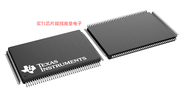
- 制造厂商:TI
- 产品类别:逻辑和电压转换
- 技术类目:专用逻辑 IC - FIFO 内存 IC
- 功能描述:16384 x 36 同步 FIFO 存储器
- 点击这里打开及下载SN74V3680的技术文档资料
- TI代理渠道,提供当日发货、严格的质量标准,满足您的目标价格

The SN74V3640, SN74V3650, SN74V3660, SN74V3670, SN74V3680, and SN74V3690 are exceptionally deep, high-speed CMOS, first-in first-out (FIFO) memories, with clocked read and write controls and a flexible bus-matching ×36/×18/×9 data flow. These FIFOs offer several key user benefits:
- Flexible ×36/×18/×9 bus matching on both read and write ports
- The period required by the retransmit operation is fixed and short.
- The first-word data-latency period, from the time the first word is written to an empty FIFO to the time it can be read, is fixed and short.
- High-density offerings up to 1 Mbit
Bus-matching synchronous FIFOs are particularly appropriate for network, video, signal processing, telecommunications, data communications, and other applications that need to buffer large amounts of data and match buses of unequal sizes.
Each FIFO has a data input port (Dn) and a data output port (Qn), both of which can assume 36-bit, 18-bit, or 9-bit width, as determined by the state of external control pins’ input width (IW), output width (OW), and bus matching (BM) during the master-reset cycle.
The input port is controlled by write-clock (WCLK) and write-enable (WEN\) inputs. Data is written into the FIFO on every rising edge of WCLK when WEN\ is asserted. The output port is controlled by read-clock (RCLK) and read-enable (REN\) inputs. Data is read from the FIFO on every rising edge of RCLK when REN\ is asserted. An output-enable (OE\) input is provided for 3-state control of the outputs.
The frequencies of the RCLK and WCLK signals can vary from 0 to fMAX, with complete independence. There are no restrictions on the frequency of one clock input with respect to the other.
There are two possible timing modes of operation with these devices: first-word fall-through (FWFT) mode and standard mode.
In FWFT mode, the first word written to an empty FIFO is clocked directly to the data output lines after three transitions of the RCLK signal. REN\ need not be asserted for accessing the first word. However, subsequent words written to the FIFO do require a low on REN\ for access. The state of the FWFT/SI input during master reset determines the timing mode.
For applications requiring more data-storage capacity than a single FIFO can provide, the FWFT timing mode permits depth expansion by chaining FIFOs in series (i.e., the data outputs of one FIFO are connected to the corresponding data inputs of the next). No external logic is required.
In standard mode, the first word written to an empty FIFO does not appear on the data output lines unless a specific read operation is performed. A read operation, which consists of activating REN\ and enabling a rising RCLK edge, shifts the word from internal memory to the data output lines.
These FIFOs have five flag pins: empty flag or output ready (EF\/OR\), full flag or input ready (FF\/IR\), half-full flag (HF), programmable almost-empty flag (PAE\), and programmable almost-full flag (PAF\). The EF\ and FF\ functions are selected in standard mode. The IR\ and OR\ functions are selected in FWFT mode. HF\, PAE\, and PAF\ are always available for use, regardless of timing mode.
PAE\ and PAF\ can be programmed independently to switch at any point in memory. Programmable offsets determine the flag-switching threshold and can be loaded by parallel or serial methods. Eight default offset settings are also provided, so that PAE\ can be set to switch at a predefined number of locations from the empty boundary. The PAF\ threshold also can be set at similar predefined values from the full boundary. The default offset values are set during master reset by the state of the FSEL0, FSEL1, and LD\.
For serial programming, SEN\, together with LD\, loads the offset registers via the serial input (SI) on each rising edge of WCLK. For parallel programming, WEN\, together with LD\, loads the offset registers via Dn on each rising edge of WCLK. REN\, together with LD\, can read the offsets in parallel from Qn on each rising edge of RCLK, regardless of whether serial parallel offset loading has been selected.
During master reset (MRS\), the read and write pointers are set to the first location of the FIFO. The FWFT pin selects standard mode or FWFT mode.
Partial reset (PRS\) also sets the read and write pointers to the first location of the memory. However, the timing mode, programmable-flag programming method, and default or programmed offset settings existing before partial reset remain unchanged. The flags are updated according to the timing mode and offsets in effect. PRS\ is useful for resetting a device in mid-operation, when reprogramming programmable flags would be undesirable.
Also, the timing modes of PAE\ and PAF\ outputs can be selected. Timing modes can be set to be either asynchronous or synchronous for PAE\ and PAF\.
If the asynchronous PAE\/PAF\ configuration is selected, PAE\ is asserted low on the low-to-high transition of RCLK. PAE\ is reset to high on the low-to-high transition of WCLK. Similarly, PAF\ is asserted low on the low-to-high transition of WCLK, and PAF\ is reset to high on the low-to-high transition of RCLK.
If the synchronous PAE\/PAF\ configuration is selected , the PAE\ is asserted and updated on the rising edge of RCLK only, and not WCLK. Similarly, PAF\ is asserted and updated on the rising edge of WCLK only, and not RCLK. The mode desired is configured during master reset by the state of the programmable flag mode (PFM).
The retransmit function allows data to be reread from the FIFO more than once. A low on the retransmit (RT\) input during a rising RCLK edge initiates a retransmit operation by setting the read pointer to the first location of the memory array. Zero-latency retransmit timing mode can be selected using the retransmit timing mode (RM). During master reset, a low on RM selects zero-latency retransmit. A high on RM during master reset selects normal latency.
If zero-latency retransmit operation is selected, the first data word to be retransmitted is placed on the output register, with respect to the same RCLK edge that initiated the retransmit, if RT\ is low.
See Figures 11 and 12 for normal latency retransmit timing. See Figures 13 and 14 for zero-latency retransmit timing.
The devices can be configured with different input and output bus widths (see Table 1).
A big-endian/little-endian data word format is provided. This function is useful when data is written into the FIFO in long-word (×36/×18) format and read out of the FIFO in small-word (×18/×9) format. If big-endian mode is selected, the most significant byte (MSB) (word) of the long word written into the FIFO is read out of the FIFO first, followed by the least-significant byte (LSB). If little-endian format is selected, the LSB of the long word written into the FIFO is read out first, followed by the MSB. The mode desired is configured during master reset by the state of the big-endian/little-endian (BE\) pin (see Figure 4 for the bus-matching byte arrangement).
The interspersed/noninterspersed parity (IP) bit function allows the user to select the parity bit in the word loaded into the parallel port (D0-Dn) when programming the flag offsets. If interspersed-parity mode is selected, the FIFO assumes that the parity bit is located in bit positions D8, D17, D26, and D35 during the parallel programming of the flag offsets. If noninterspersed-parity mode is selected, D8, D17, and D26 are assumed to be valid bits and D32, D33, D34, and D35 are ignored. Interspersed parity mode is selected during master reset by the state of the IP input. Interspersed parity control has an effect only during parallel programming of the offset registers. It does not affect data written to and read from the FIFO.
The SN74V3640, SN74V3650, SN74V3660, SN74V3670, SN74V3680, and SN74V3690 are fabricated using high-speed submicron CMOS technology, and are characterized for operation from 0°C to 70°C.
- Choice of Memory Organizations
- SN74V3640 - 1024 × 36 Bit
- SN74V3650 - 2048 × 36 Bit
- SN74V3660 - 4096 × 36 Bit
- SN74V3670 - 8192 × 36 Bit
- SN74V3680 - 16384 × 36 Bit
- SN74V3690 - 32768 × 36 Bit
- 166-MHz Operation (6-ns Read/Write Cycle Time)
- User-Selectable Input and Output Port Bus Sizing
- ×36 in to ×36 out
- ×36 in to ×18 out
- ×36 in to ×9 out
- ×18 in to ×36 out
- ×9 in to ×36 out
- Big-Endian/Little-Endian User-Selectable Byte Representation
- 5-V-Tolerant Inputs
- Fixed, Low, First-Word Latency
- Zero-Latency Retransmit
- Master Reset Clears Entire FIFO
- Partial Reset Clears Data, but Retains Programmable Settings
- Empty, Full, and Half-Full Flags Signal FIFO Status
- Programmable Almost-Empty and Almost-Full Flags; Each Flag Can Default to One of Eight Preselected Offsets
- Selectable Synchronous/Asynchronous Timing Modes for Almost-Empty and Almost-Full Flags
- Program Programmable Flags by Either Serial or Parallel Means
- Select Standard Timing (Using EF\ and FF\ Flags) or First-Word Fall-Through (FWFT) Timing (Using OR\ and IR\ Flags)
- Output Enable Puts Data Outputs in High-Impedance State
- Easily Expandable in Depth and Width
- Independent Read and Write Clocks Permit Reading and Writing Simultaneously
- High-Performance Submicron CMOS Technology
- Available in 128-Pin Thin Quad Flat Pack (TQFP)
- Supply voltage (Min) (V)
- 3.15
- Supply voltage (Max) (V)
- 3.45
- Input type
- Standard CMOS
- Output type
- 3-State
- Clock Frequency (Max) (MHz)
- 1
- Features
- Programmable Flags, Unidirectional
SN74V3680的完整型号有:SN74V3680-15PEU、SN74V3680-6PEU,以下是这些产品的关键参数及官网采购报价:
SN74V3680-15PEU,工作温度:0 to 70,封装:LQFP (PEU)-128,包装数量MPQ:72个,MSL 等级/回流焊峰值温度:Level-3-260C-168 HR,引脚镀层/焊球材料:NIPDAU,TI官网SN74V3680-15PEU的批量USD价格:18.711(1000+)
SN74V3680-6PEU,工作温度:0 to 70,封装:LQFP (PEU)-128,包装数量MPQ:72个,MSL 等级/回流焊峰值温度:Level-3-260C-168 HR,引脚镀层/焊球材料:NIPDAU,TI官网SN74V3680-6PEU的批量USD价格:21.919(1000+)


